

Color filter array alignment mark formation in backside illuminated image sensors
a technology of color filter array and image sensor, which is applied in the field of processing techniques for forming backside illuminated image sensors, can solve the problems of affecting the fill factor and quantum efficiency of image sensors, failing to adequately address the alignment of backside features with frontside features, and it is difficult under conventional practice to align backside features such as color filter elements of cfa with frontside features. , to achieve the effect of improving image sensor die size or cost, improving performance and improving the alignment of
- Summary
- Abstract
- Description
- Claims
- Application Information
AI Technical Summary
Benefits of technology
Problems solved by technology
Method used
Image

Examples
Embodiment Construction
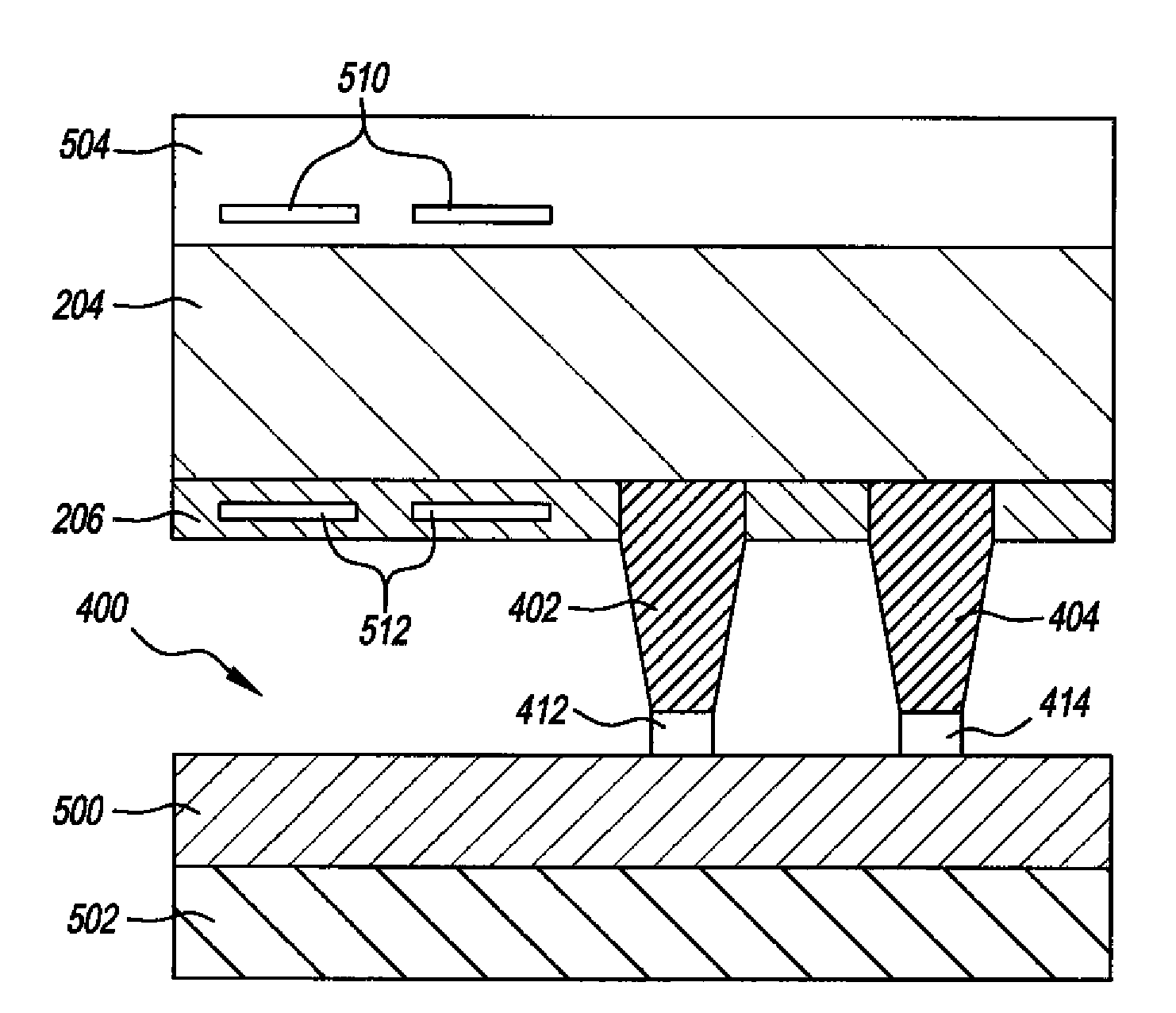
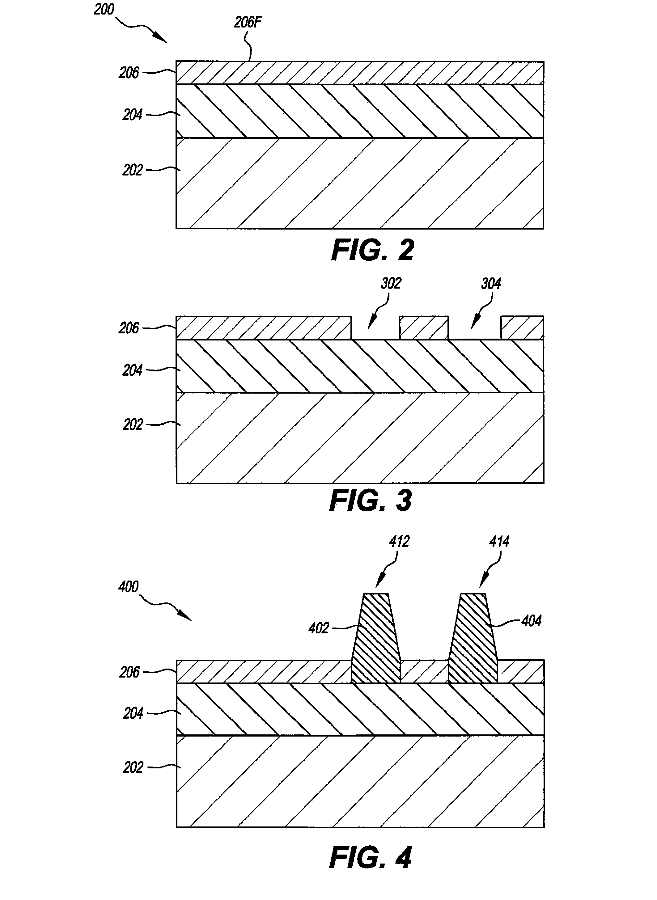
[0019]The present invention will be illustrated herein in conjunction with particular embodiments of digital cameras, backside illuminated image sensors, and processing techniques for forming such image sensors. It should be understood, however, that these illustrative arrangements are presented by way of example only, and should not be viewed as limiting the scope of the invention in any way. Those skilled in the art will recognize that the disclosed arrangements can be adapted in a straightforward manner for use with a wide variety of other types of imaging devices and image sensors.
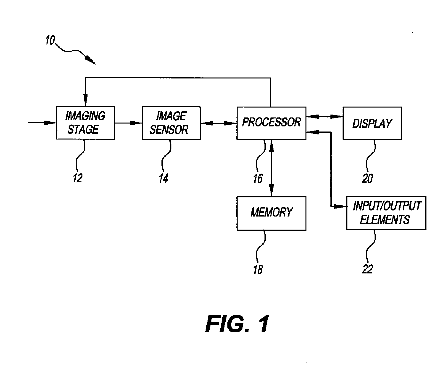
[0020]FIG. 1 shows a digital camera 10 in an illustrative embodiment of the invention. In the digital camera, light from a subject scene is input to an imaging stage 12. The imaging stage may comprise conventional elements such as a lens, a neutral density filter, an iris and a shutter. The light is focused by the imaging stage 12 to form an image on an image sensor 14, which converts the incident ligh...
PUM
 Abstract
Description
Claims
Application Information