Check patentability & draft patents in minutes with Patsnap Eureka AI!

One-time programmable memory device and fabrication method thereof

a memory device and one-time technology, applied in the field of one-time programmable memory devices, can solve the problems of complex manufacturing methods of prior art otp memory devices

Active Publication Date: 2022-06-14
HEFECHIP CORP LTD
View PDF4 Cites 0 Cited by
  • Summary
  • Abstract
  • Description
  • Claims
  • Application Information

AI Technical Summary

Problems solved by technology

However, the prior art OTP memory device utilizing PN polysilicon junctions or PN single crystalline silicon junctions require complicate layouts and circuit, and the manufacturing method for making the prior art OTP memory device is complex.

Method used


Image

  • One-time programmable memory device and fabrication method thereof
  • One-time programmable memory device and fabrication method thereof
  • One-time programmable memory device and fabrication method thereof

Examples


Embodiment Construction

[0040]It is to be noted that the following descriptions of preferred embodiments of this invention are presented herein for purposes of illustration and description only; it is not intended to be exhaustive or to be limited to the precise form disclosed.

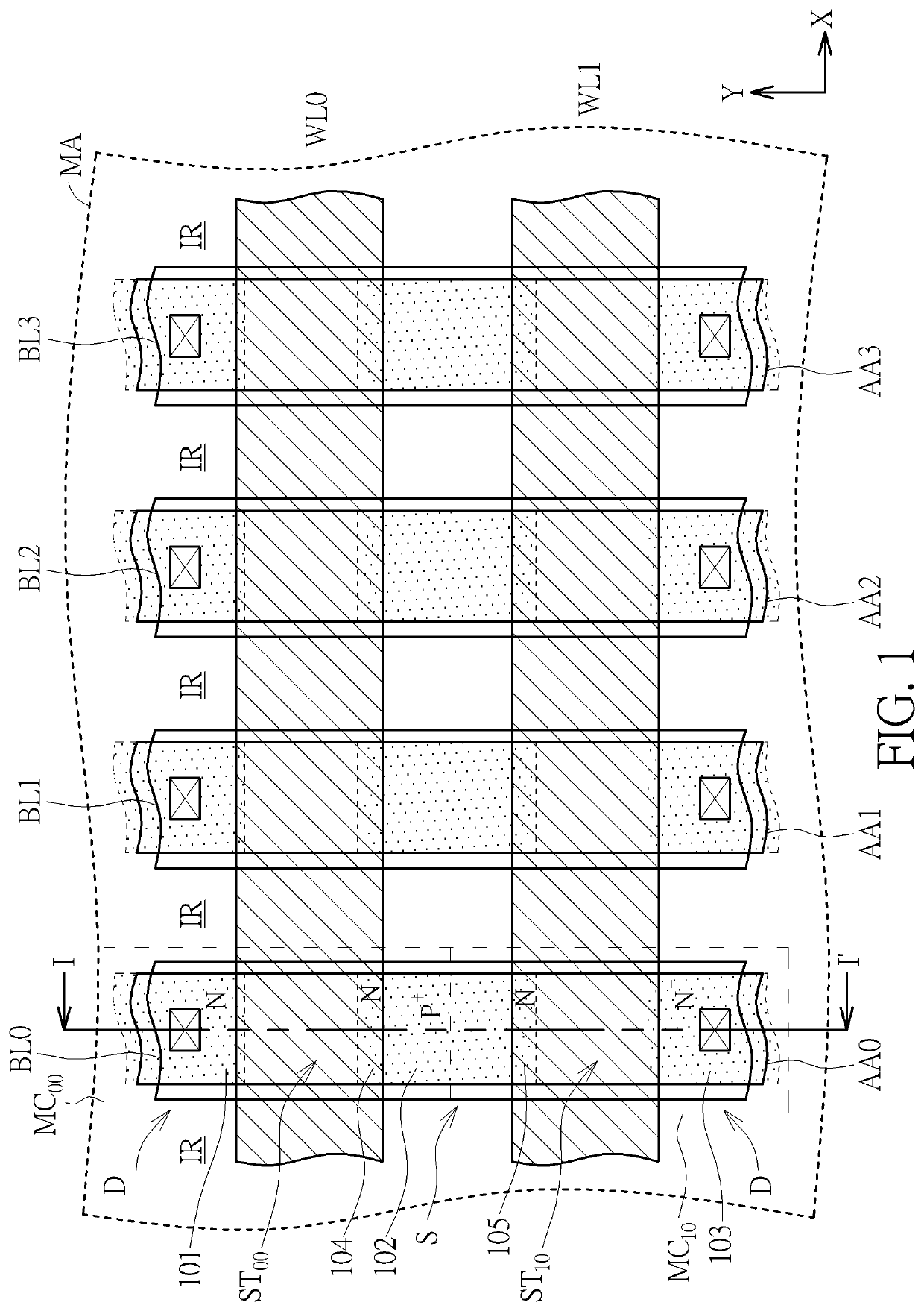
[0041]The present invention pertains to a semiconductor memory device, such as a one-time programmable (OTP) memory cell (OTP memory cell or OTP cell), including a transistor and a diode. The transistor may be a planar MOS transistor, a Fin FET, a gate all around (GAA) transistor, etc. The diode is a PN junction diode. The OTP cell further comprises a substrate having a first conductivity type, and a source and a drain in the substrate. The source includes a source doping region having the first conductivity type. The drain includes a drain doping region having a second conductivity type opposite to the first conductivity type. A gate is disposed on the substrate between the source and the drain. The source further includes a pocket ...


PUM

PropertyMeasurementUnit
gate voltageaaaaaaaaaa
tile angleaaaaaaaaaa

Abstract

A semiconductor memory device includes at least an OTP cell having a transistor and a PN junction diode. The OTP cell further includes a substrate having a first conductivity type, and a source and a drain in the substrate. The source includes a source doping region having the first conductivity type. The drain includes a drain doping region having a second conductivity type opposite to the first conductivity type. A gate is disposed on the substrate between the source and the drain. The source further includes a pocket doping region having the second conductivity type under the gate. The pocket doping region and the source doping region constitute the PN junction diode.

Description

BACKGROUND OF THE INVENTION1. Field of the Invention[0001]The present disclosure relates to a semiconductor memory device. More particularly, the present disclosure relates to a one-transistor one-diode (1T1D) one-time programmable (OTP) memory device and a method for fabricating the same.2. Description of the Prior Art[0002]One-time programmable (OTP) memory devices that contain electrical fuse are known in the art. To program the OTP memory device, a high voltage can be applied to induce a high current to flow through the electrical fuse of the OTP memory device such that the OTP memory device can be programmed or burned into a high or low resistance state (depending on either fuse or anti-fuse). Typically, the electrical fuse is a programmable resistive device that can be constructed from a segment of interconnect such as polysilicon.[0003]However, the prior art OTP memory device utilizing PN polysilicon junctions or PN single crystalline silicon junctions require complicate layo...

Claims


Application Information

Patent Timeline
Patent Type & Authority Patents(United States)
IPC IPC(8): G11C16/04H01L27/112H01L21/265G11C17/06
CPCH01L27/11206G11C17/06H01L21/26513H01L21/26586G11C17/16G11C17/18H01L23/5252H01L29/7391H10B20/20
Inventor CHERN, GEENG-CHUAN
Owner HEFECHIP CORP LTD
Features
  • R&D
  • Intellectual Property
  • Life Sciences
  • Materials
  • Tech Scout
  • Unparalleled Data Quality
  • Higher Quality Content
  • 60% Fewer Hallucinations
Learn More