
Electrically alterable non-volatile memory with n-bits per cell

a non-volatile memory, electric altering technology, applied in static storage, digital storage, instruments, etc., can solve the problems of unstable reference voltage level, complex sensing scheme of multi-level memory devices, and requiring 2.sup.n-1 voltage references

Inactive Publication Date: 2001-07-05
BTG INT LTD
View PDF0 Cites 2 Cited by
  • Summary
  • Abstract
  • Description
  • Claims
  • Application Information

AI Technical Summary

Problems solved by technology

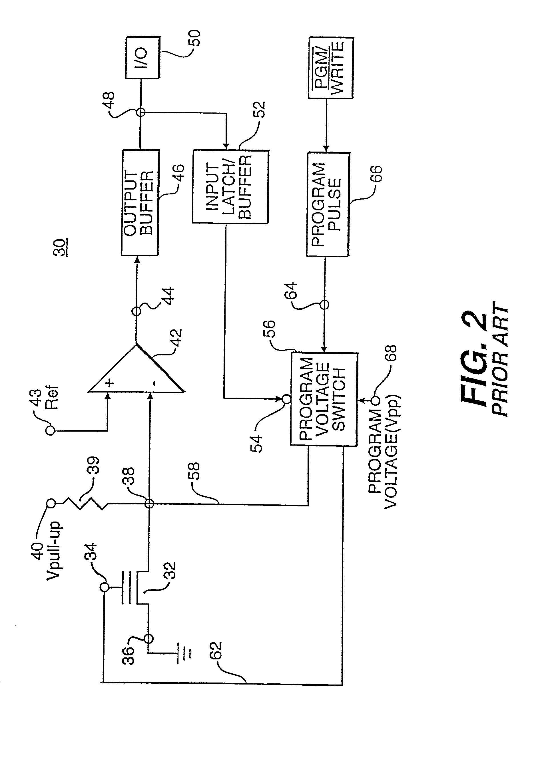
Sensing schemes for multi-level memory devices are more complex and require 2.sup.n-1 voltage references.
A limitation with the conventional sensing schemes is often inaccurate and unstable reference voltage levels.
The conventional sensing schemes have reference voltage levels which cannot accurately track bit line voltage levels through process, temperature, and voltage variations.
All of these approaches have the common characteristic that whatever information is stored on such a memory cell is volatile because such a cell loses its data whenever power is removed.
Furthermore, these types of memory cells must be periodically refreshed as they have a tendency to lose charge over time even when power is maintained.

Method used


Image

  • Electrically alterable non-volatile memory with n-bits per cell
  • Electrically alterable non-volatile memory with n-bits per cell
  • Electrically alterable non-volatile memory with n-bits per cell

Examples


Embodiment Construction

[0066] A multi-level (or multi-bit) memory device which contains more than one bit of information per memory cell needs accurate and stable reference voltages. The reference voltages allow a multi-level memory cell to be correctly read over various process, voltage, and temperature ranges. The reference voltages must be implemented into the integrated circuit which can accurately sense the multi-level voltage levels of the memory cells as well as track each memory array voltage level as it drifts with the process, voltage, and temperature variations. An unstable or inaccurate reference voltage tends to cause problems such as an improper voltage level read of a bit line, and the like from a memory cell.

[0067] In a 2-bit per memory cell embodiment, the memory cell includes four voltage levels V0, V1, V2, and V3 at each of the bit lines as illustrated by FIG. 15. To uniquely detect each of the four voltage levels, it is necessary to generate at least three reference voltages, each of t...


PUM


Abstract

A multi-bit memory device with a memory cell means for storing input information for an indefinite period of time. The multi-bit memory means stores information in up to Kn memory states (Kn>1). A memory cell programming means and comparator means is also included. The present multi-bit memory device also includes a voltage divider arrangement with pull-up devices in a memory array to provide stable and accurate reference voltages over process, temperature, and voltage variations.

Description

[0001] This application is a continuation-in-part of U.S. patent application Ser. No. 08 / 071,816, filed Jun. 4, 1993 entitled "Electrically Alterable Non-Volatile Memory with N-Bits Per Memory Cell," which is a continuation of U.S. patent application Ser. No. 07 / 652,878, filed Feb. 8, 1991 (now U.S. Pat. No. 5,218,569) entitled "Electrically Alterable Non-Volatile Memory with N-Bits Per Cell."[0002] 1. Field of the Invention[0003] This invention relates to non-volatile memory (NVM) devices; and, more particularly, is concerned with an apparatus and method for providing a multi-level NVM device with stable reference voltages.[0004] 2. Description of the Background Art[0005] In conventional single-bit per cell memory devices, the memory cell assumes one of two information storage states, either an "on" state or an "off" state. This combination of either "on" or "off" defines one bit of information. As a result, a memory device which can store n-bits of data requires n separate memory ...

Claims


Application Information

Patent Timeline
Patent Type & Authority Applications(United States)
IPC IPC(8): G11C11/56
CPCG11C7/1006G11C11/5621G11C11/5628G11C11/5642G11C16/12G11C16/16G11C16/32G11C16/3454G11C16/3459G11C2211/5621G11C2211/5634G11C2211/5642G11C11/56
Inventor BANKS, GERALD J.
Owner BTG INT LTD
Learn More