Method of fabrication of a microstructure having an internal cavity

a microstructure and internal cavity technology, applied in the field of fabricating a microstructure having an inside cavity, can solve the problems of difficult electrical contact, incompatibility with these boundary conditions, and limited applicability, and achieve excellent hermetic seal of the cavity and facilitate the making of the indent

Inactive Publication Date: 2002-01-03
TILMANS HENDRIKUS A C +2
View PDF0 Cites 103 Cited by
  • Summary
  • Abstract
  • Description
  • Claims
  • Application Information

AI Technical Summary

Benefits of technology

[0012] The present invention is directed to a microstructure product and a method of fabricating a microstructure having an internal cavity. Preferably, the covity is sealed with a controlled ambient allowing a free choice of the sealing gas composition and the sealing pressure or vacuum.[0013] The method preferably does not require special equipment to perform the fabrication of such microstructures in a vacuum or controlled inert gas ambient.[0014] The method is suited for micro-electromechanical systems (MEMS) packaging wherein all the process steps are compatible with packaging equipment.

Problems solved by technology

A common drawback of these techniques is that they are rather limited in applicability, since device separation is difficult (the device has been made on one of the two wafers).
It is also difficult to create electrical contacts.
There are applications that are not compatible with these boundary conditions of temperature and flatness.
Furthermore, the technique of anodic bounding also requires flat surfaces and needs the application of a high voltage in order to achieve the bonding.
Finally, the technique of gluing does not provide a real hermetic bond.

Method used


Image

  • Method of fabrication of a microstructure having an internal cavity
  • Method of fabrication of a microstructure having an internal cavity
  • Method of fabrication of a microstructure having an internal cavity

Examples


Embodiment Construction

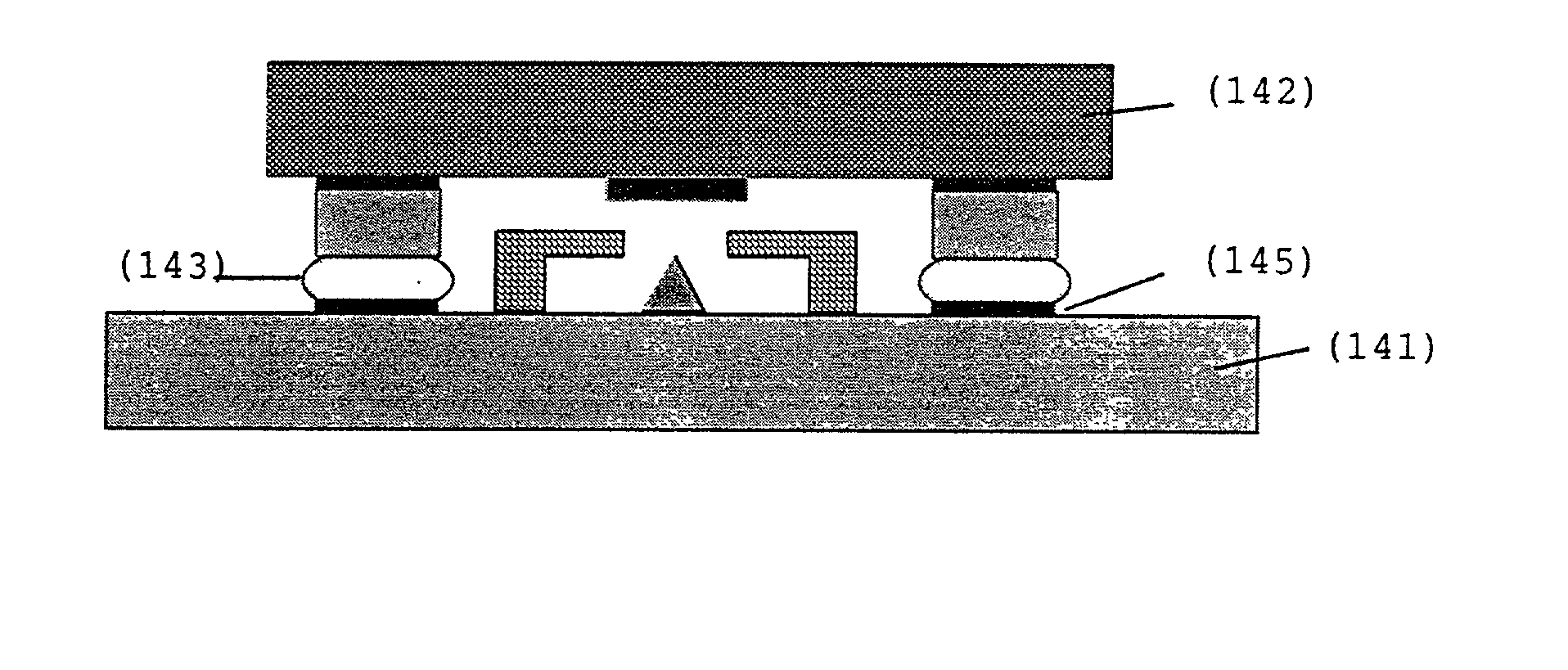
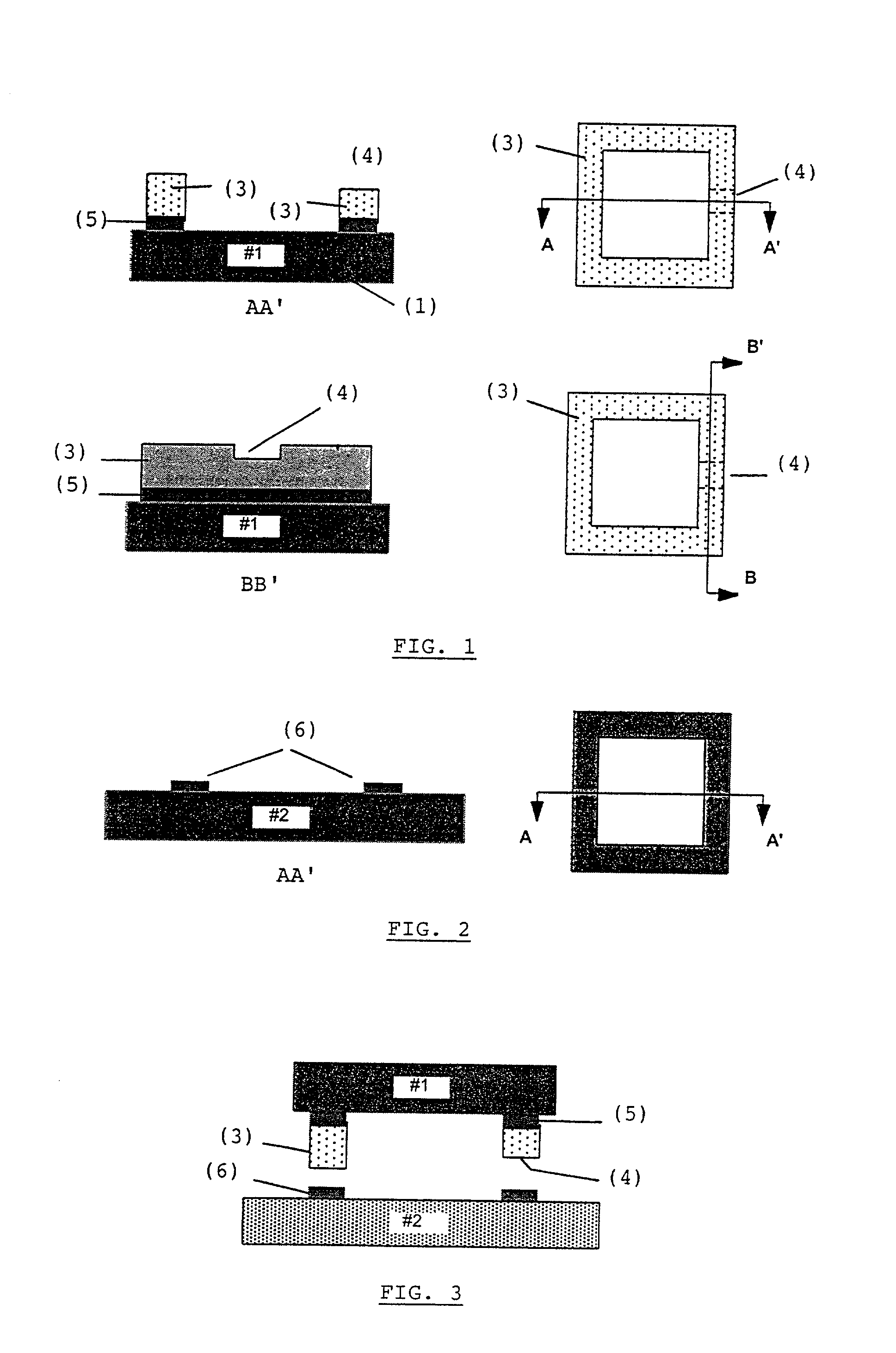
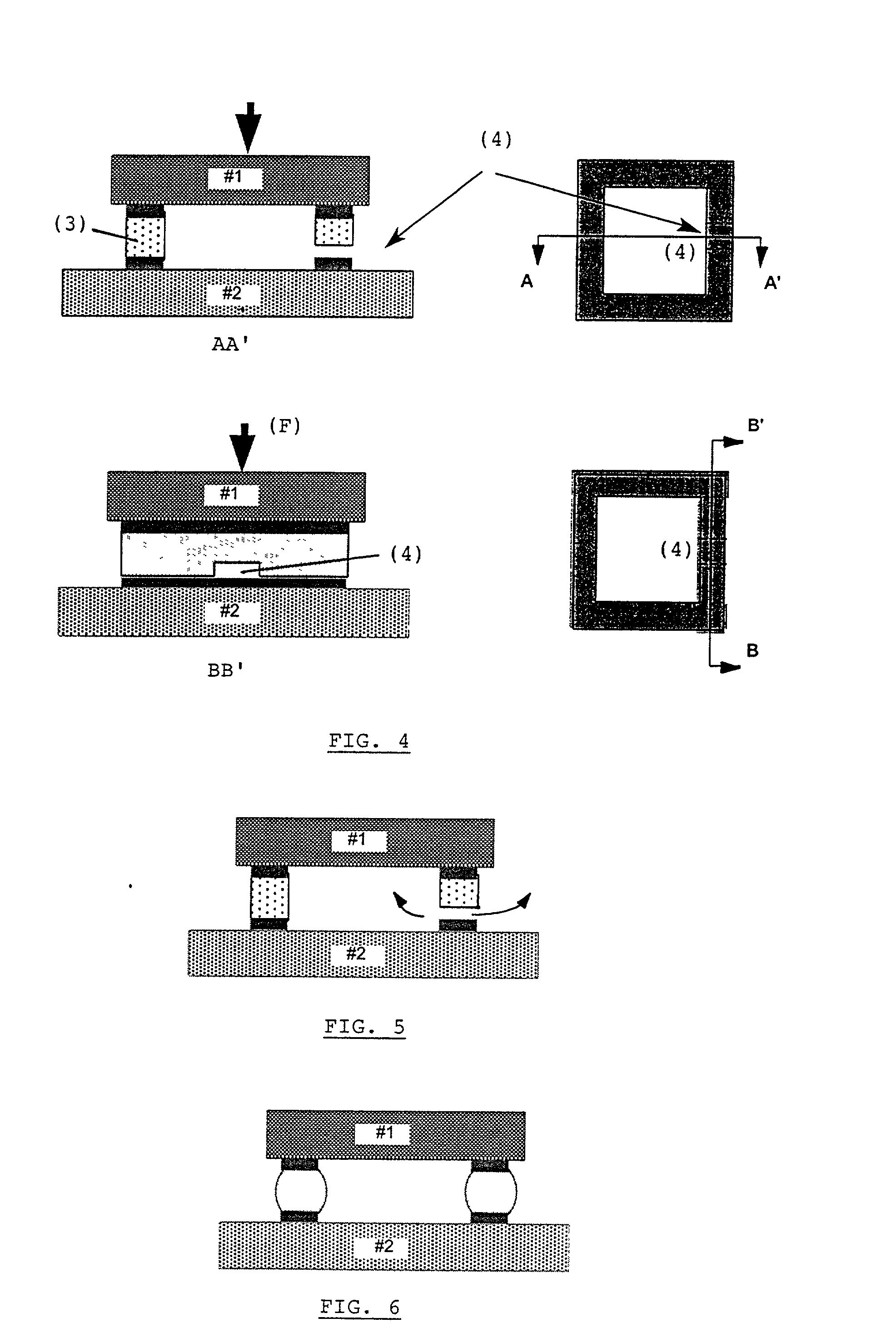
[0076] An integral design and fabrication approach incorporating all the key elements of a micro-relay, i.e., actuator, electrical contacts, housing of the electrical contacts, structural design, micro-machining fabrication process and packaging, has resulted in the micro-relay schematically shown in FIG. 16. The heart of the micro-relay comprises two "flip-chip assemblied" chips (161) using the method of the present invention described hereabove.

[0077] The assembly process is based on the eutectic (162) bonding between electroplated tin lead (SnPb) and gold (Au) layers. One of the two chips of the assembly uses a ferromagnetic substrate (161) and comprises a U-core electromagnet, consisting of a double-layer Cu coil (cross section Cu winding 6.times.8 .mu.m.sup.2, total number of turns N=127), electroplated NiFe (50 / 50) poles (1.times.0.15 mm.sup.2), and the lower electrical contact. The upper chip (162) uses an oxidised silicon substrate. The chip accomodates an armature consistin...


PUM

PropertyMeasurementUnit
temperatureaaaaaaaaaa
thickaaaaaaaaaa
temperaturesaaaaaaaaaa

Abstract

The present invention relates to a method of fabricating a microstructure having an inside cavity comprising the steps of: depositing a first layer or a first stack of layers in a substantially closed geometric configuration on a first substrate; performing an indent on the first layer or on the top layer of said first stack of layers; depositing a second layer or a second stack of layers substantially with said substantially closed geometric configuration on a second substrate; aligning and bonding said first substrate on said second substrate such that a microstructure having a cavity is formed according to said closed geometry configuration.

Description

[0001] The present invention is related to a microstructure product and a method of fabricating of a microstructure having an internal and preferably sealed cavity.[0002] The present invention is also related to specific applications of this method of fabricating of a microstructure.[0003] Microstructures having an internal cavity can be formed by making an assembly of two chips or two wafers or a chip-on-wafer with a spacer in-between. Such structures should have hermetically sealed cavities filled with a controlled ambient (gas composition and / or pressure).[0004] These structures can be used for many different applications such as microaccelerometers, microgyroscopes, microtubes, vibration microsensors, micromirrors, micromechanical resonators or "resonant strain gauges", micromechanical filters, microswitches and microrelays.[0005] Traditionally, for these applications, the ambient of the cavity is defined during the assembly of the several components by anodic, fusion or eutecti...

Claims


Application Information

Patent Timeline
Patent Type & Authority Applications(United States)
IPC IPC(8): B81B7/00G01L9/00G01P15/08G01P15/125H01H1/00H01H35/14H01L23/02H03H3/007B81C1/00
CPCB81B7/0077B81C1/00293G01J5/045G01L9/0042G01L9/0073G01P15/0802G01P15/125H01H1/0036H01H35/14H01L2224/16H01L2924/01025H01L2924/01077H01L2924/01078H01L2924/01079H03H9/1057H01L23/10H01L21/50H01L2924/01322H01L2924/01327H01L2924/00
Inventor TILMANS, HENDRIKUS A.C.BEYNE, ERICVAN DE PEER, MYRIAM
Owner TILMANS HENDRIKUS A C
Why Eureka
Try Eureka