Semiconductor integrated circuit and printed wiring substrate provided with the same

Inactive Publication Date: 2002-01-24
CANON KK
View PDF0 Cites 38 Cited by
  • Summary
  • Abstract
  • Description
  • Claims
  • Application Information

AI Technical Summary

Benefits of technology

0007] It is an object of the present invention to solve the above-noted problem and to provide a semiconductor integrated circuit having the arrangement of array-like electrode pads which can effectively dis

Problems solved by technology

Therefore, when as represented by recent CPU's and microprocessors, the higher speed of the operating frequency of the semiconductor integrated circuit is remarkably progressing, there arises the problem that the radiation noise of electromagnetic waves from the printed wi

Method used


Image

  • Semiconductor integrated circuit and printed wiring substrate provided with the same
  • Semiconductor integrated circuit and printed wiring substrate provided with the same
  • Semiconductor integrated circuit and printed wiring substrate provided with the same

Examples


first embodiment

[0016] (First Embodiment)

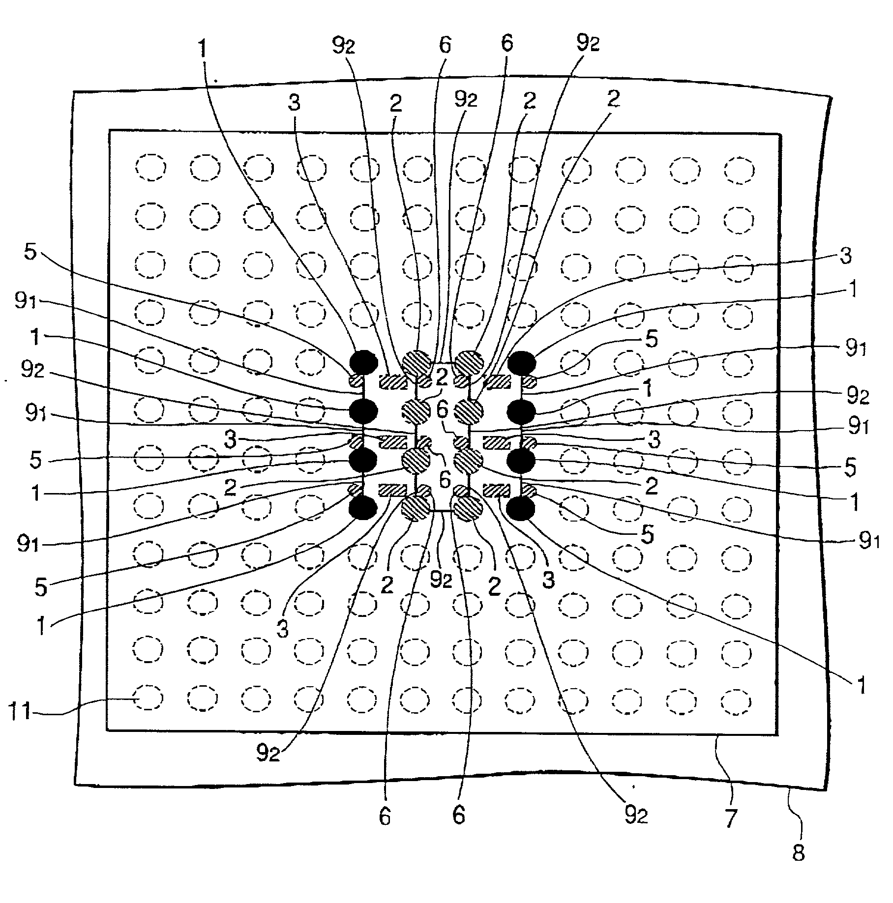
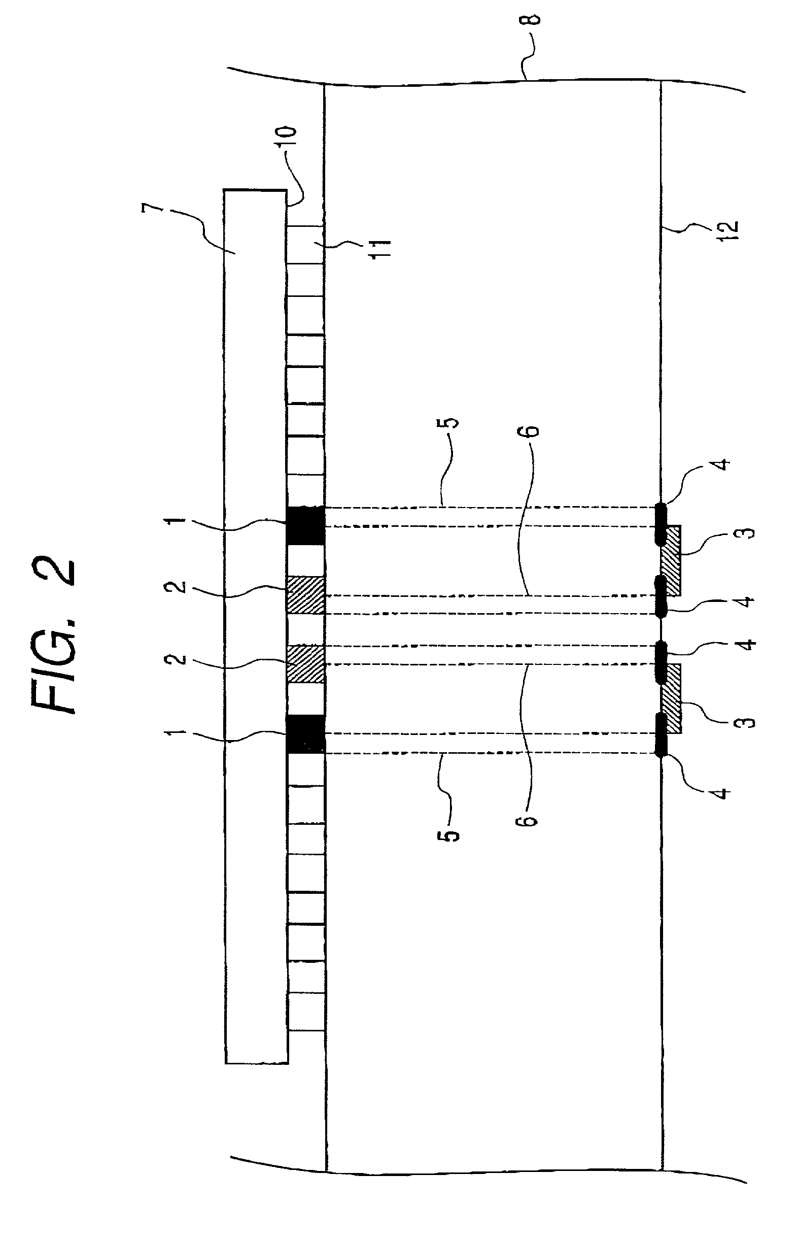
[0017] FIG. 1 is a plan view of a printed wiring substrate carrying thereon a semiconductor integrated circuit according to a first embodiment of the present invention, and FIG. 2 is a longitudinal cross-sectional view of the printed wiring substrate of FIG. 1. FIG. 1 shows the printed wiring substrate 8 carrying thereon the semiconductor integrated circuit 7 having array-like electrode pads as it is seen from a surface on which the semiconductor integrated circuit 7 is mounted.

[0018] In the bottom surface 10 of the package of the semiconductor integrated circuit 7, a plurality of connecting electrode pads 11 (in FIG. 1, indicated by dotted circles) for making the electrical connection between the semiconductor integrated circuit 7 and an external circuit are regularly arranged at a full grid in a grid-like fashion. Of the connecting electrode pads 11, electrode pads 1 for ground (indicated by black painted-out circles) are connecting electrode pads for grou...

second embodiment

[0023] (Second Embodiment)

[0024] FIG. 3 is a plan view of a printed wiring substrate carrying thereon a semiconductor integrated circuit according to a second embodiment of the present invention. In this embodiment, as shown in FIG. 3, the power supply electrode pads 2 of the semiconductor integrated circuit 7 of FIGS. 1 and 2 are disposed on the innermost side and the electrode pads 1 for ground are disposed so as to surround the power supply electrode pads 2, and all of the power supply electrode pads 2 and all of the electrode pads 1 for ground are connected by a wiring pattern 9.sub.2 and a wiring pattern 9.sub.1, respectively. In the other points, the construction of the present embodiment is the same as that of the first embodiment.

[0025] Again in such a construction, as in the first embodiment, the radiation noise of electromagnetic waves from the printed wiring substrate 8 is reduced and the drawing-out of the wiring from the electrode pads for signals to the surrounding par...

third embodiment

[0026] (Third Embodiment)

[0027] FIG. 4 is a plan view of a printed wiring substrate carrying thereon a semiconductor integrated circuit according to a third embodiment of the present invention. This embodiment is such that in the first embodiment, the electrode pads 1 for ground and the power supply electrode pads 2 are disposed in spirally opposed relationship with each other and in the other points, the construction of the present embodiment is the same as that of the first embodiment.

[0028] Again in such a construction, as in the first embodiment, the radiation noise of electromagnetic waves from the printed wiring substrate 8 is reduced and the drawing-out of the wiring from the electrode pads for signals to the surrounding parts becomes easy, and this is also effective for the higher density of the printed wiring substrate.


PUM

PropertyMeasurementUnit
Densityaaaaaaaaaa
Shapeaaaaaaaaaa

Abstract

When a semiconductor integrated circuit having a plurality of electrode pads disposed in an array-like form on the bottom surface thereof is mounted on a printed wiring substrate, a plurality of ground electrode pads and a plurality of power supply electrode pads are concentratedly arranged on the central portion of the semiconductor integrated circuit mounted on the printed wiring substrate so as to constitute groups so as to be opposed to each other, and a decoupling capacitor is mounted on the opposite surface of the printed wiring substrate through a through-hole, whereby the creation of radiation noise is suppressed and the higher density of the printed wiring substrate is achieved.

Description

BACKGROUND OF THE INVENTION[0001] 1. Field of the Invention[0002] This invention relates to a semiconductor integrated circuit having a plurality of electrode pads disposed in an array-like form on the bottom surface thereof, and a printed wiring substrate having the semiconductor integrated circuit mounted thereon.[0003] 2. Related Background Art[0004] In recent years, the circuit scale of a semiconductor integrated circuit has grown larger and larger. As the circuit scale of the semiconductor integrated circuit has grown larger, the number of pins necessary for the connection of the integrated circuit and an external circuit has been increased and therefore, an IC package having a plurality of electrode pads disposed in an array-like form on the bottom surface thereof has been developed. Since it is a semiconductor integrated circuit, the electrode pads disposed in an array-like form on the bottom surface thereof include a power supply electrode pad for supplying a power source to...

Claims


Application Information

Patent Timeline
IPC IPC(8): H01L23/52H01L21/3205H01L21/60H01L21/82H01L21/822H01L23/64H01L27/04H05K1/02H05K1/18
CPCH01L23/642H01L2224/16H01L2924/19106H05K1/0231H05K2201/10545H05K2201/10734B61C17/04B61D17/005C08F283/02C08K3/22C08K5/14C08K5/17C08L67/00Y02T30/00
Inventor TAKEUCHI, YASUSHI
Owner CANON KK
Why Eureka
Try Eureka