Method of producing spacer and method of manufacturing image forming apparatus

a technology of image forming apparatus and spacer, which is applied in the manufacture of electrode systems, electrode assembly, electric discharge tube/lamps, etc., can solve the problems of less heat-melting of substrates, distorted images, and fear of creeping discharge on the surface of spacers

Inactive Publication Date: 2002-03-14
CANON KK
View PDF8 Cites 21 Cited by
  • Summary
  • Abstract
  • Description
  • Claims
  • Application Information

AI Technical Summary

Problems solved by technology

Even when many cold-cathode devices are arranged on a substrate with a high density, the problem of heat-melting the substrate less occurs.
First, the electrons emitted from the electron emitting device near the spacer adhere to the spacer, or ions ionized by the action of the emitted electrons adhere to the spacer to possibly charge the spacer. Therefore, the orbits of the electrons emitted from the electron emitting device are bent due to charge of the spacer, and thus the electrons reach positions deviated from normal positions on the fluorescent material provided on the faceplate, thereby displaying a distorted image near the spacer.
Secondary, a high voltage Va of several hundreds V or more (for example, a high electric field of 1 kV/mm or more) is applied between the rear plate and the faceplate to accelerate the electrons emitted from the electron emitting device, thereby causing a fear of creeping discharge on the surface of the spacer. Particularly, when the spacer is charged as described above, there is the probability that discharge is induced.
However, in some types of images, i.e., in cases in which the driving pulse width is increased to increase the amount of the electrons emitted, the distortion of an image cannot be sufficiently decreased only by the method of removing charge by using the high-resistance film.
This failure in potential control significantly influences the vicinity of the cathode because of its low electron kinetic energy.
Furthermore, when a cylindrical spacer, a columnar spacer having a polygonal sectional shape, or a plate-like spacer having uneven side surfaces is used as the spacer base member, as shown in FIGS. 5A and B, it is very difficult to remove the spaces between the bundled spacers.
In this case, when contact between the film non-formation portion and the film material is inhibited, contact between the film formation portion and the film material is liable to be insufficient.
On the other hand, when the film material is sufficiently put into contact with the film formation portion, contact between the film non-formation portion and the film material causes a problem.
This is because it is difficult to control the conditions for providing the film material on a surface of the spacer base member between the bundled spacer base members, wherein the surface of the spacer base member will be supposed to face a surface of the adjacent spacer base member each other when the plurality of the spacer base members are bundled.
Namely, the production method can pre...

Method used


Image

  • Method of producing spacer and method of manufacturing image forming apparatus
  • Method of producing spacer and method of manufacturing image forming apparatus
  • Method of producing spacer and method of manufacturing image forming apparatus

Examples


example 1

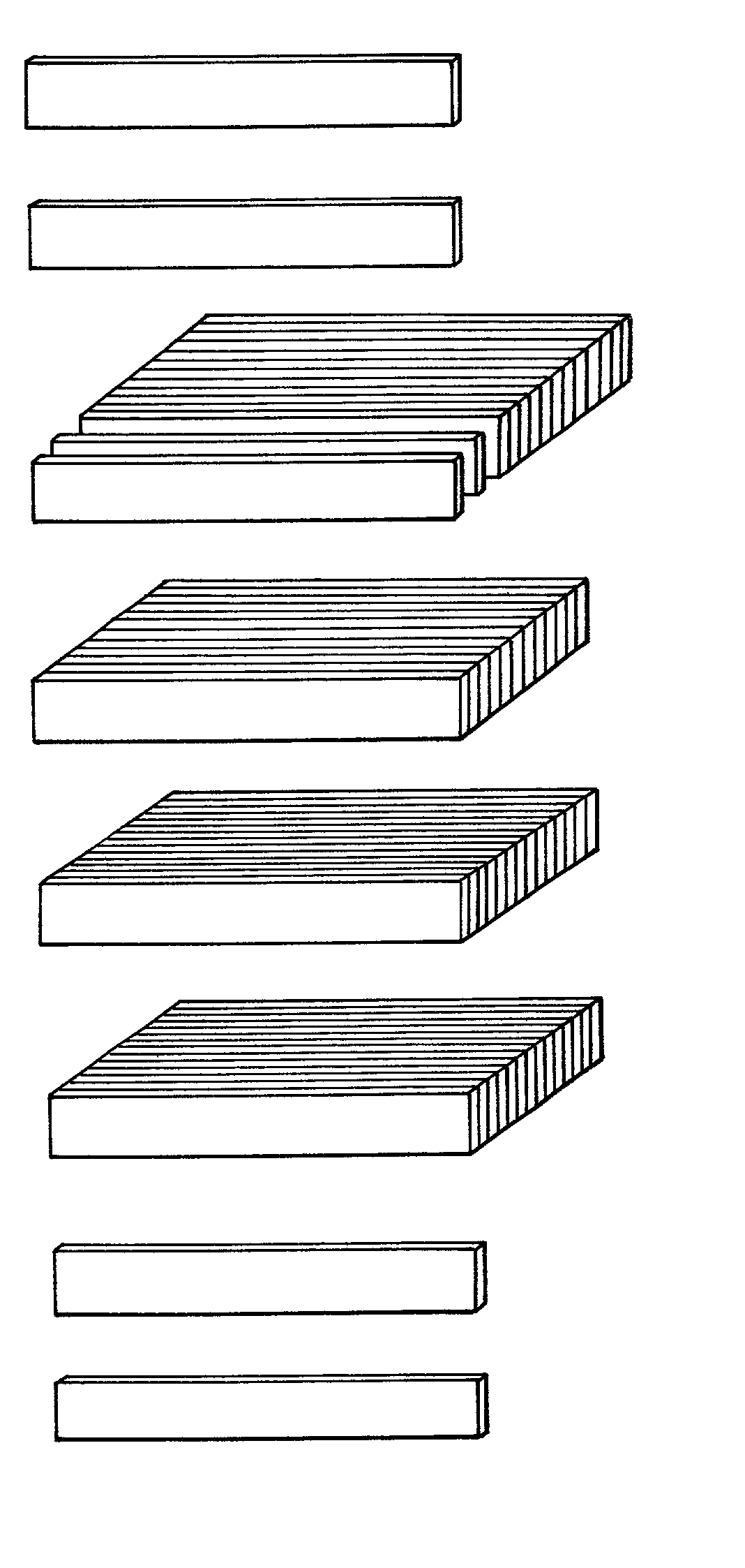
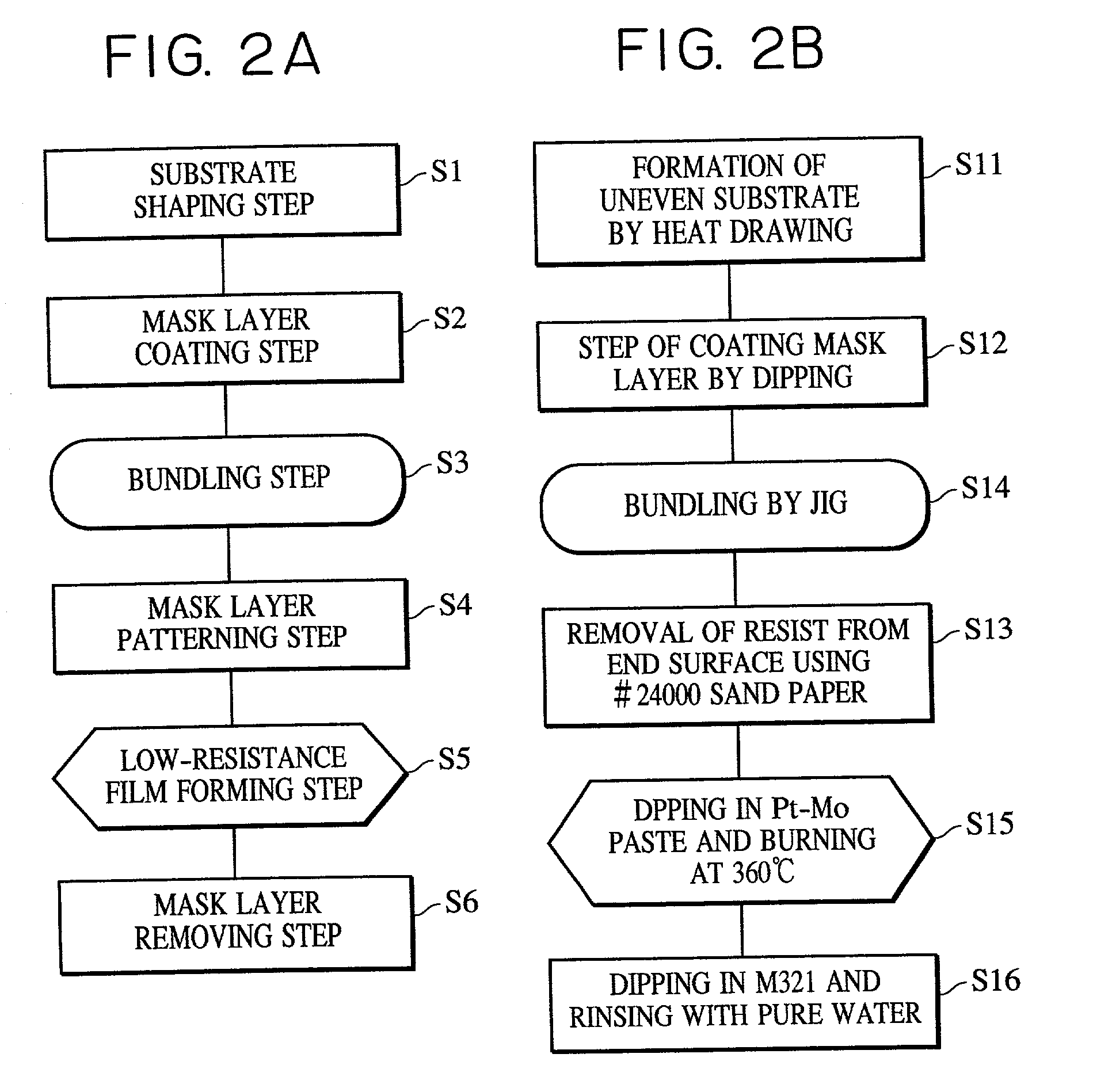
[0286] The spacer 20 used in example 1 was formed as described below. The procedure for the substrate shaping step, the mask layer forming step, the bundling step, the mask layer patterning step, low-resistance film forming step and the mask layer removing step was the same as show in FIG. 2B. FIG. 30 schematically shows spacer base materials and substrates in each of the steps in this procedure.

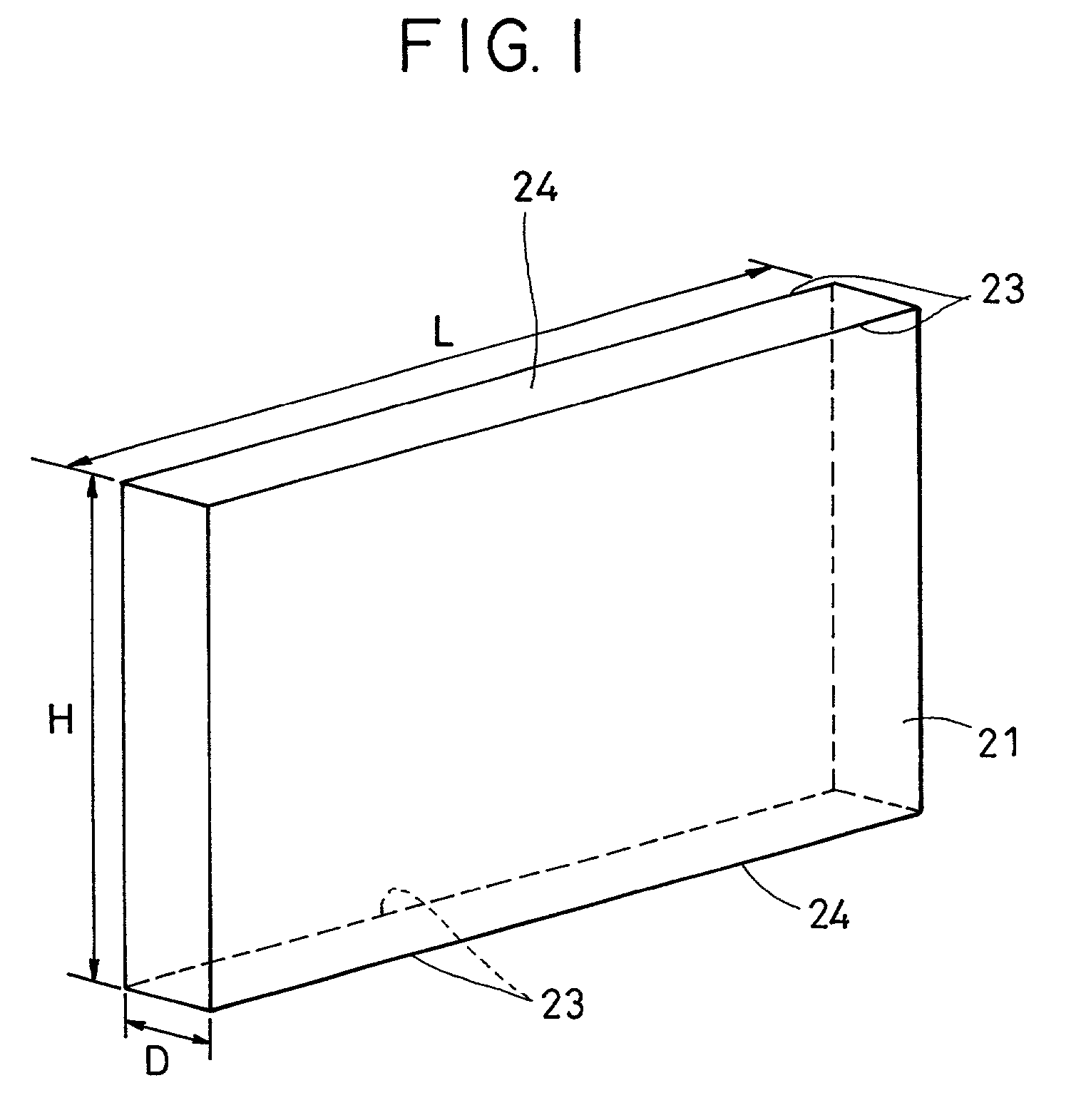
[0287] A soda lime glass plate comprising the same material as the faceplate and rear plate was used as a spacer base material, and subjected to the heat drawing process shown in FIG. 13 to obtain the spacer base member 21 having the sectional shape shown in FIGS. 9B and 10B. FIG. 10 is an enlarged sectional view of one of the ends near the contact portions shown in FIG. 9.

[0288] The thus-obtained spacer base member 21 was used as the spacer 20. The spacer base member 21 formed in this example had a height H of 3 mm, a thickness D of 0.2 mm, a length L of 650 mm, as shown in FIG. 1. The glas...

example 2

[0305] The spacer 20 used in this example was produced as described above. The method of patterning the low-resistance film of the spacer base member 21 was performed according to the procedure for the substrate shaping step, the mask layer forming step, the bundling step, the mask layer patterning step, the low-resistance film forming step, and the mask layer removing step shown in FIG. 3B. FIG. 31A to G show the appearance of a substrate in the respective forming steps. The same substrate shaping step and the same forming method as Example 1 were repeated except that the bundling step was performed after the mask layer pattering step to form the low-resistance film (electrode) 25 on the end surfaces (contact surfaces) of the spacer base member 21.

[0306] Furthermore, the high-resistance film 22 was formed by the same sputtering method as Example 1 to form the spacer 20.

[0307] In each of the thus-obtained spacers 20, the low-resistance film (electrode) 25 had light reflection, the s...

example 3

[0309] The spacer 20 used in this example was produced as described below. The low-resistance film (electrode) 25 was formed by the same method as Example 1 except that a plate-shaped spacer base member 21 having contact portions each having the shape shown in FIG. 9 and 10, and an uneven stripe structure in the longitudinal direction was used in place of the spacer base member 21 formed in Example 1. Also, the bundling step was performed by the same method as Example 1 before the mask layer pattering step after the formation of the mask layer. In this step, the bundle state is shown on the left side of FIG. 5A (not showing the coated mask layer). In this state, spaces occurred near the contact portions. Then, the high-resistance film 22 was formed by sputtering in the same manner as Example 1 to produce the spacer 20.

[0310] In each of the thus-obtained spacers 20, the low-resistance film (electrode) 25 had light reflection, the shape with good linearity, and neither projection to t...


PUM

PropertyMeasurementUnit
Electrical resistanceaaaaaaaaaa
Sheet resistanceaaaaaaaaaa

Abstract

The present invention provides a method of producing a spacer provided between a first substrate and a second substrate on which an electron emitting device is arranged, the method including the step of forming a film on at least a portion of at least one surface of the spacer. The film forming step includes the step of preparing a bundle of a plurality of spacer base members, and the step of coating a film material on the bundle, and wherein the bundle on which the film material is coated has a mask layer for covering at least a film non-formation portion near the film formation portion of each of the plurality of spacer base members of the bundle.

Description

[0001] 1. Field of the Invention[0002] The present invention relates to a method of producing a spacer arranged between a pair of substrates, and a method of manufacturing an image forming apparatus using the spacer.[0003] 2. Description of the Related Art[0004] Known electron emitting devices include the two types of devices including a hot-cathode device and a cold-cathode device. Of these devices, known examples of the cold-cathode device include a surface conduction-type emission device, a field emission device (referred to as a FE type" hereinafter) and a metal / insulating layer / metal type emission device (referred to as a MIM type" hereinafter).[0005] Examples of the surface conduction-type emission device include the device disclosed in M. I. Elinson, Radio Eng. Electron Phys., 10, 1290 (1965), and the other devices described below.[0006] The surface conduction-type emission device utilizes the phenomenon that electrons are emitted by passing an electric current through a smal...

Claims


Application Information

Patent Timeline
IPC IPC(8): H01J9/24H01J9/18H01J29/86
CPCH01J9/185H01J9/242H01J29/864H01J2329/863H01J2329/8635H01J2329/864H01J2329/8645H01J2329/8655H01J2329/866H01J2329/8665
Inventor ITO, NOBUHIROFUSHIMI, MASAHIRO
Owner CANON KK
Why Eureka
Try Eureka