
Completely thin-film based composite dispersion compensating structure and its method of use

a composite dispersion and compensating structure technology, applied in the field of complete thin-film based composite dispersion compensating structure and its, can solve the problems of fiber dispersion becoming an increasingly important problem, affecting the performance of composite dispersion,

Inactive Publication Date: 2002-04-18
JABLONSKI MARK KENNETH +4
View PDF0 Cites 46 Cited by
  • Summary
  • Abstract
  • Description
  • Claims
  • Application Information

AI Technical Summary

Problems solved by technology

In such systems, fiber dispersion will become an increasingly important problem.
Presently, second order dispersion has become a huge problem and with it various compensation approaches have been proposed, whose effects we will soon see.
However, with respect to light wave transmission, the dispersion tolerances have become very strict.
This spreading out of the pulses ultimately interferes with the detection capability of the receiver, as pulses overlap with their neighbors.
This phenomenon of third-order dispersion becomes a serious problem with increasing bit-rates and distances, as the required accuracy for detection becomes greater.
For example, in systems using bit rates of 10 Gbps (10 gigabits every second) and greater, this phenomenon is a serious worry, and for 40 Gbps and greater systems [over distances of only 80 km], the worry is even greater.
Therefore, for future high-speed optical communication systems, it will become difficult to use today's normal fiber systems.
There have been many attempts at compensating for third-order dispersion, but none of them have been successful enough to be realized.
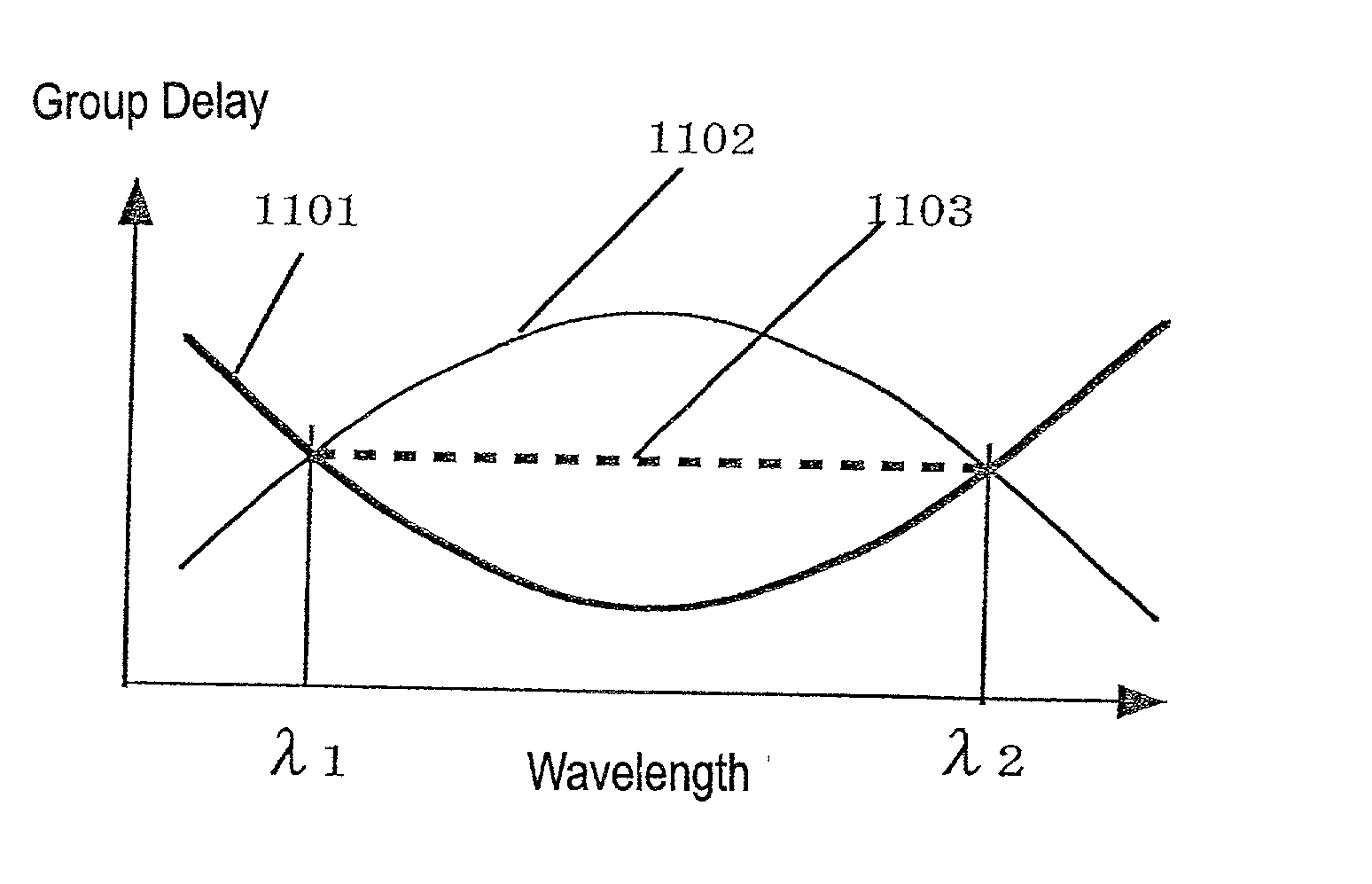
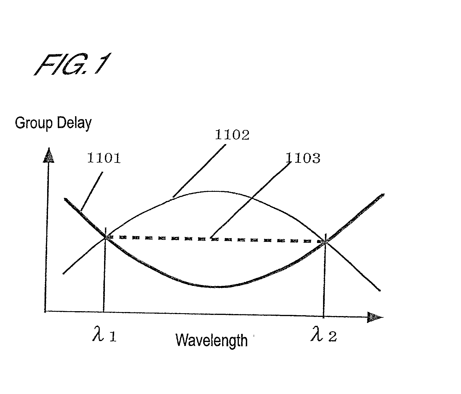
Using simply one dispersion compensation unit, it is extremely difficult to obtain a sufficiently wide bandwidth group delay characteristics, a sufficient amount of dispersion compensation, as well as complex group delay shapes.
However, an important question is how small can the loss be made, as the total loss is proportional to the number of elements, since the loss is additive.
However, for bandwidths as wide as 30 nm and 40 nm, changing the amount of dispersion compensation is difficult.
Connecting dispersion compensation units in series using collimator and lens assemblies rapidly results in a high accumulation in loss.

Method used


Image

  • Completely thin-film based composite dispersion compensating structure and its method of use
  • Completely thin-film based composite dispersion compensating structure and its method of use
  • Completely thin-film based composite dispersion compensating structure and its method of use

Examples


Embodiment Construction

[0067] The figures regarding the practical realization of the form of this invention will be referred to below. In order to understand this invention, a general outline of the components making up the device, the general shape, and arrangement of the sub-components will explained with respect to figures. Concerning the circumstances of the explanation of this invention, some figures will show magnified versions of the structures showed in other figures. Not all the realizable forms of this invention, described in this patent will have similar figures. In each figure structural parts that are the same will be labeled with the same number. Overlapping explanations may be abbreviated.

[0068] Concerning the discussion of the invention below, light dispersion compensation or simply dispersion compensation, light dispersion compensation element or simply dispersion compensation element, and light dispersion compensation method or simply dispersion compensation method are used.

[0069] In a f...


PUM


Abstract

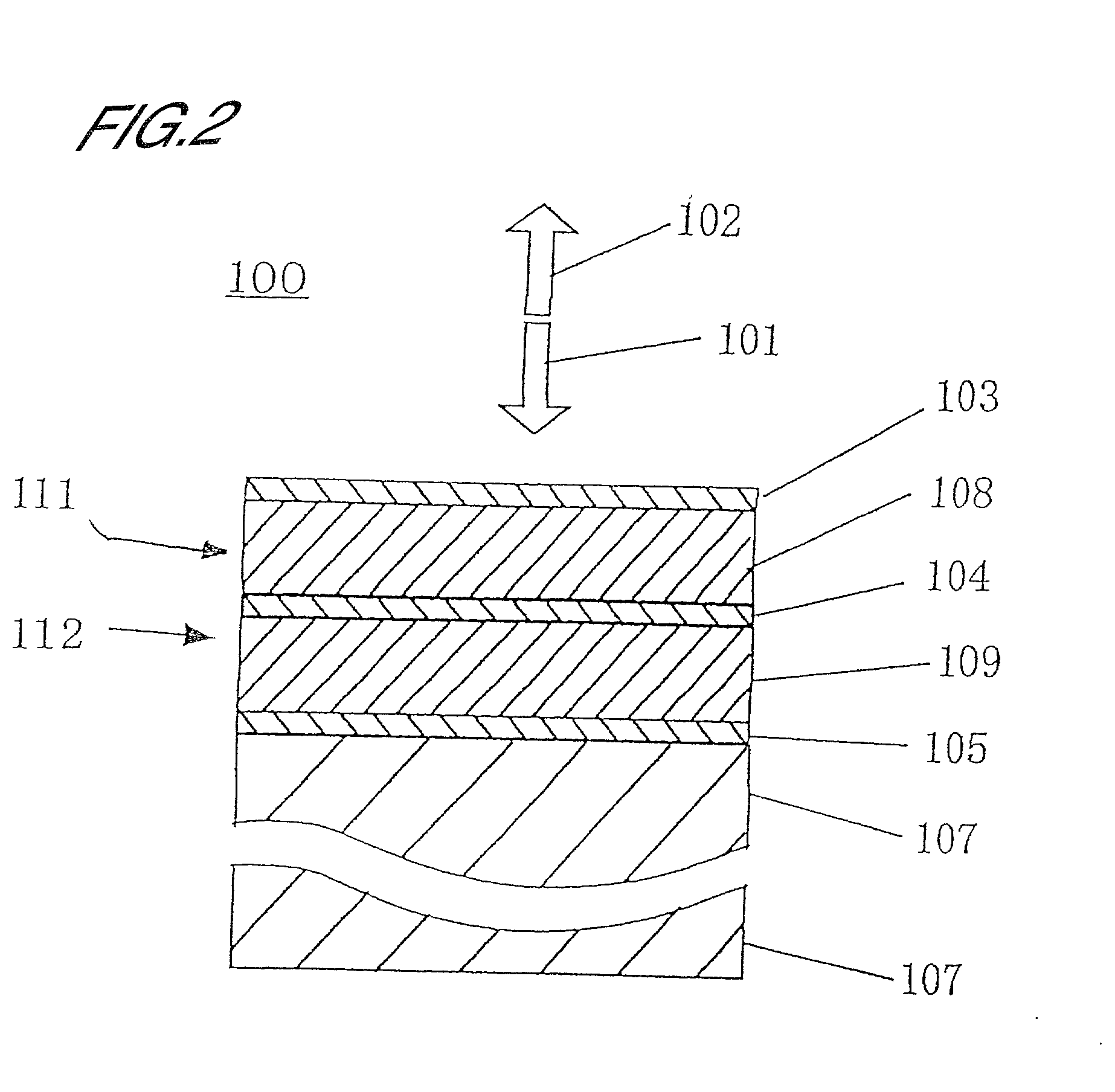
This invention, a composite dispersion compensation structure made up of at least two dispersion compensation elements in an opposing arrangement, can provide low cost dispersion compensation over a wide bandwidth by utilizing multiple reflections.

Description

[0001] 1. Field of the Invention[0002] This invention relates to a completely thin-film based composite dispersion compensating structure and it's method of use.[0003] 2. Description of Related Art[0004] It is recognized that the demand for higher bit rates and longer propagation distances in fiber optic light wave communication systems is steadily increasing. In such systems, fiber dispersion will become an increasingly important problem. Various possible dispersion compensation approaches will be tried. Presently, second order dispersion has become a huge problem and with it various compensation approaches have been proposed, whose effects we will soon see.[0005] However, with respect to light wave transmission, the dispersion tolerances have become very strict. Compensation of only second order dispersion is insufficient, rather third order dispersion must also be compensated for.[0006] Below, FIGS. 10 and 11 will be used to explain future second order dispersion compensation met...

Claims


Application Information

Patent Timeline
IPC IPC(8): G02B5/28G02B6/34H04B10/2507H04B10/2525
CPCG02B5/288G02B6/29364H04B10/25133G02B6/29367G02B6/29394G02B6/29365
Inventor JABLONSKI, MARK KENNETHKIKUCHI, KAZUROTAKUSHIMA, YUICHITANAKA, YUICHIFURUKI, KENJI
Owner JABLONSKI MARK KENNETH
Learn More