Multi-zone temperature control for semiconductor wafer

a technology of semiconductor wafers and temperature control, applied in the field of semiconductor fabrication processes and equipment, can solve the problems of uneven affecting the wafer, mechanical challenges in the processing of larger wafers, and difficulty in achieving and maintaining a uniform environment throughout the wafer during processing

Active Publication Date: 2015-07-30
TAIWAN SEMICON MFG CO LTD
View PDF14 Cites 42 Cited by
  • Summary
  • Abstract
  • Description
  • Claims
  • Application Information

AI Technical Summary

Benefits of technology

[0008]In some embodiments, an apparatus comprises a processor for receiving a plurality of measurements of a critical dimension (CD) at respective locations in a circuit pattern etched from a film comprising a film material on a first semiconductor substrate. A single wafer chamber is provided for forming a second film of the film material on a second semiconductor substrate. The single wafer chamber is responsive to a control signal from the processor to locally adjust a thickness of the second film based on the measurements of the CD.

Problems solved by technology

Processing larger wafers introduces mechanical challenges.
Because a 450 mm wafer has a larger diameter and surface area, it is more difficult to attain and maintain a uniform environment throughout the wafer while processing.
Additionally, secondary sources of heating and cooling (e.g., radiative heat transfer to or from the chamber walls) may affect the wafer unevenly.

Method used


Image

  • Multi-zone temperature control for semiconductor wafer
  • Multi-zone temperature control for semiconductor wafer
  • Multi-zone temperature control for semiconductor wafer

Examples


Embodiment Construction

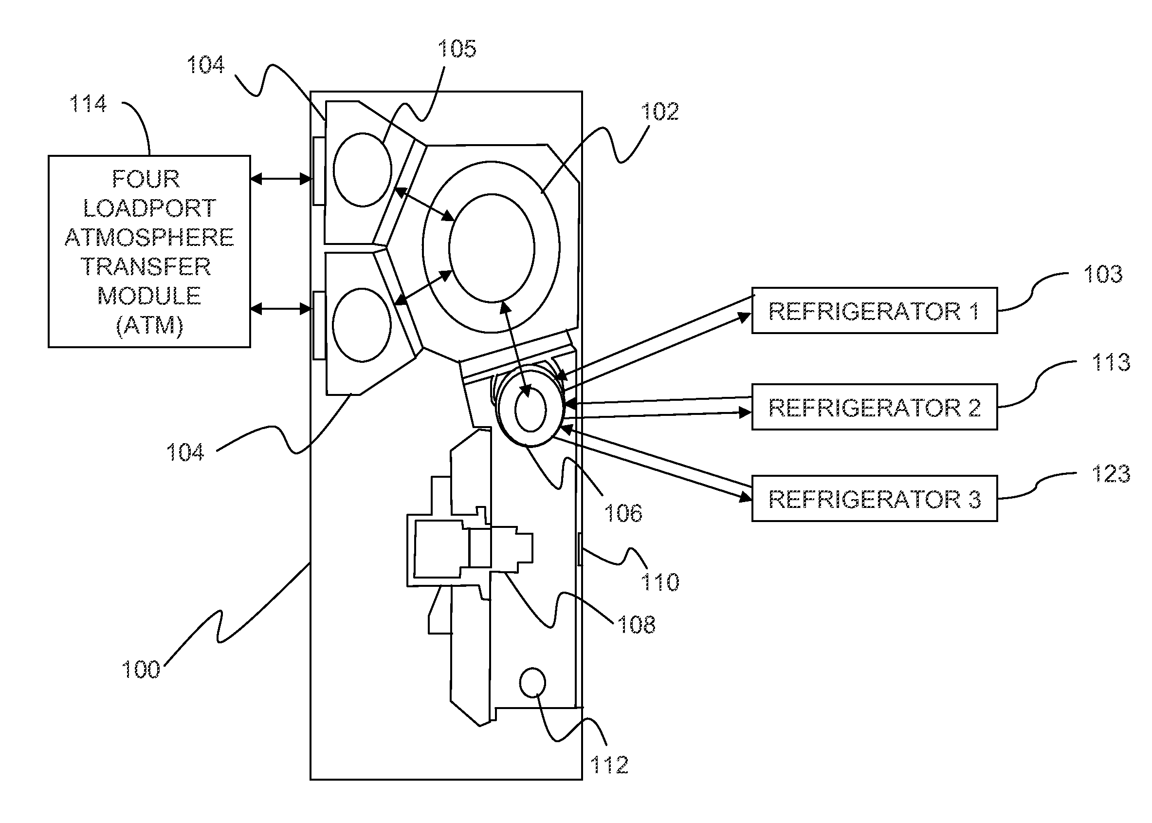
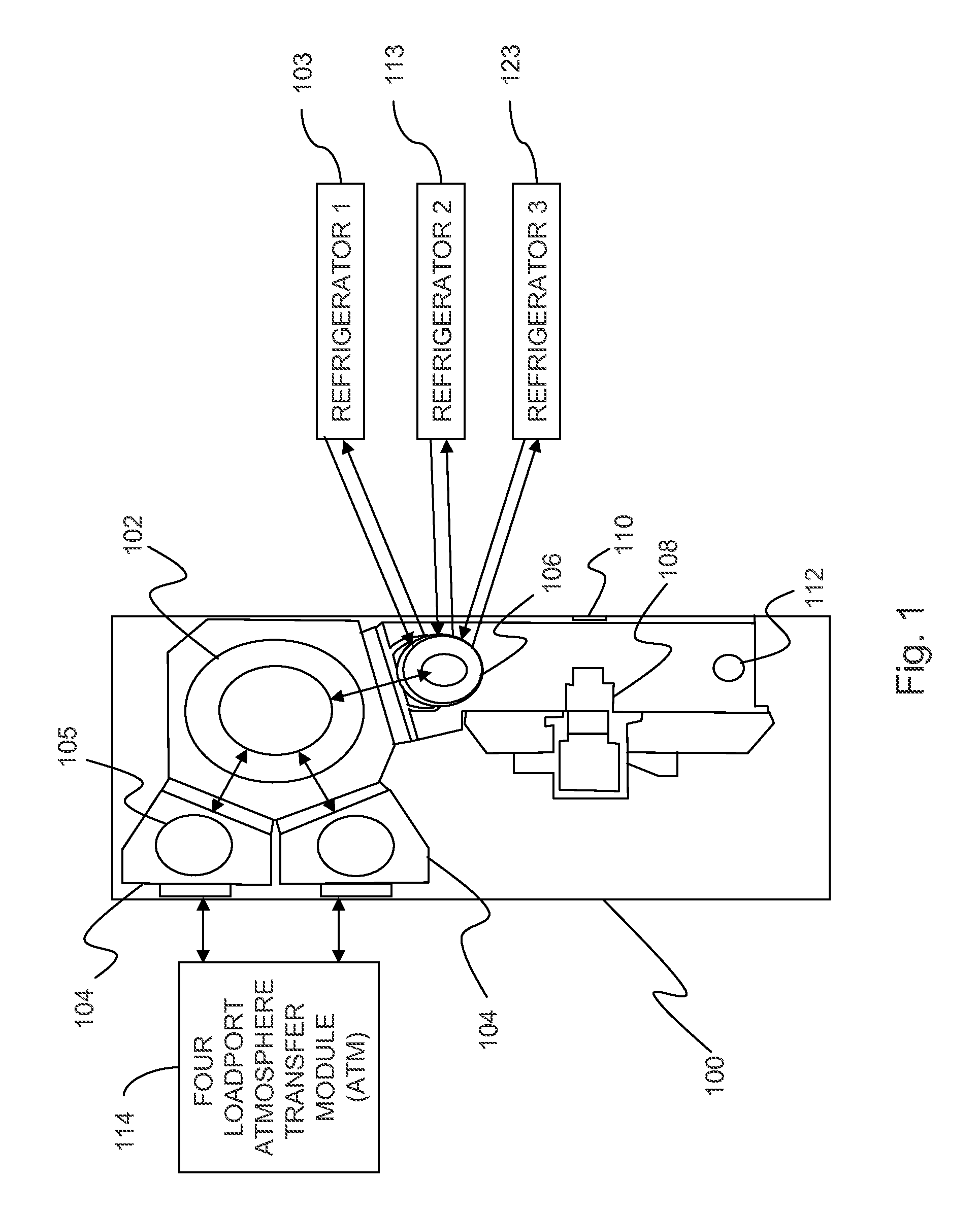
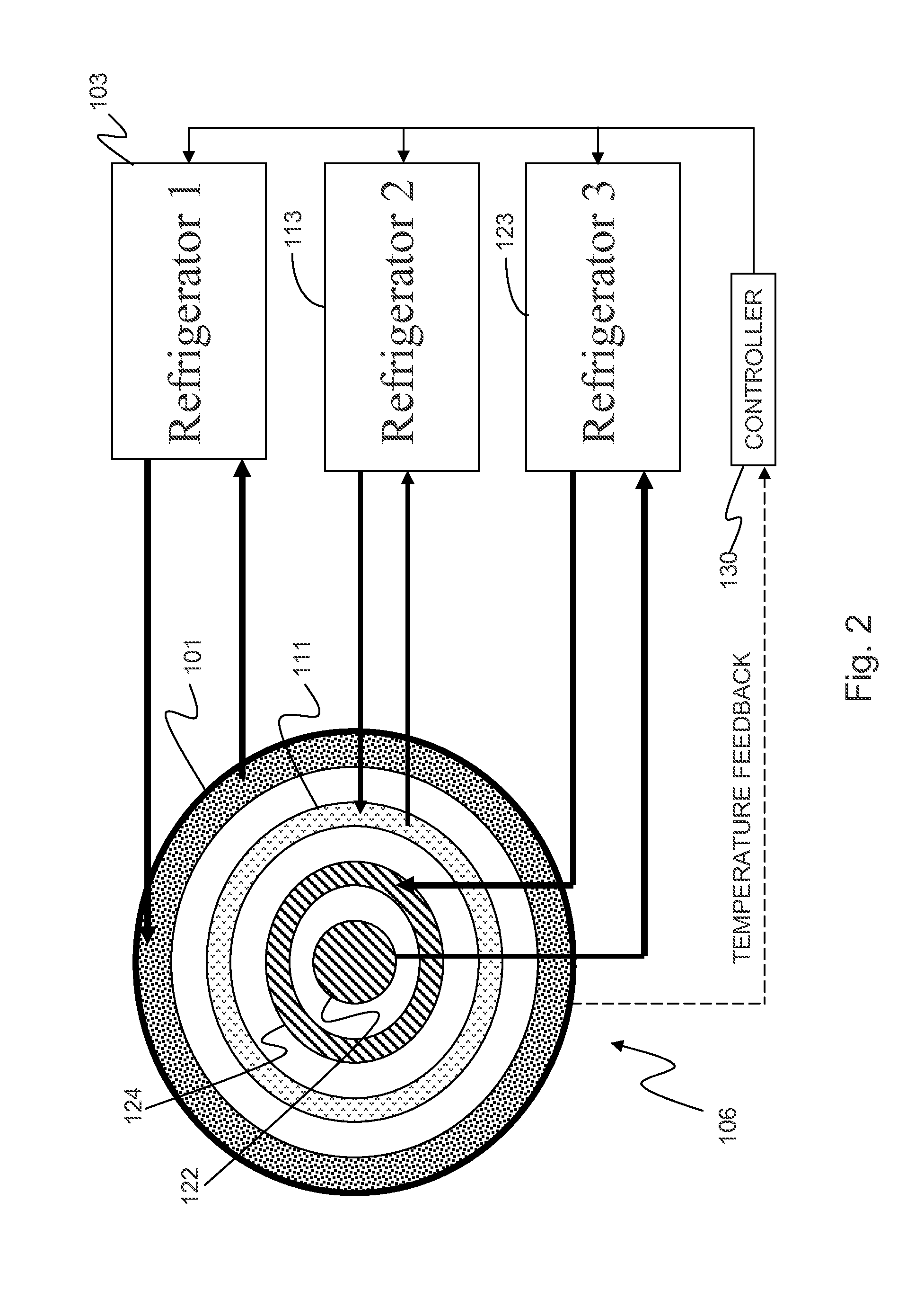
[0025]This description of the exemplary embodiments is intended to be read in connection with the accompanying drawings, which are to be considered part of the entire written description. In the description, relative terms such as “lower,”“upper,”“horizontal,”“vertical,”, “above,”“below,”“up,”“down,”“top” and “bottom” as well as derivative thereof (e.g., “horizontally,”“downwardly,”“upwardly,” etc.) should be construed to refer to the orientation as then described or as shown in the drawing under discussion. These relative terms are for convenience of description and do not require that the apparatus be constructed or operated in a particular orientation. Terms concerning attachments, coupling and the like, such as “connected” and “interconnected,” refer to a relationship wherein structures are secured or attached to one another either directly or indirectly through intervening structures, as well as both movable or rigid attachments or relationships, unless expressly described othe...


PUM

PropertyMeasurementUnit
sizeaaaaaaaaaa
diameteraaaaaaaaaa
critical dimensionaaaaaaaaaa

Abstract

An apparatus and a method for controlling critical dimension (CD) of a circuit is provided. An apparatus includes a controller for receiving CD measurements at respective locations in a circuit pattern in an etched film on a first substrate and a single wafer chamber for forming a second film of the film material on a second substrate. The single wafer chamber is responsive to a signal from the controller to locally adjust a thickness of the second film based on the measured CD's. A method provides for etching a circuit pattern of a film on a first substrate, measuring CD's of the circuit pattern, adjusting a single wafer chamber to form a second film on a second semiconductor substrate based on the measured CD. The second film thickness is locally adjusted based on the measured CD's.

Description

RELATED APPLICATIONS[0001]This application is a continuation application of U.S. patent application Ser. No. 13 / 777,212, filed on Feb. 26, 2013, which is a divisional application of U.S. patent application Ser. No. 12 / 370,746, filed on Feb. 13, 2009, the contents of each of which are incorporated herein by reference in their entirety.FIELD OF THE INVENTION[0002]The present disclosure relates to semiconductor fabrication processes and equipment.BACKGROUND[0003]The semiconductor chip fabrication industry continues to strive for reductions in costs. One of the major strategies to reduce the production cost per chip is to migrate towards the use of larger diameter semiconductor wafers. Current semiconductor foundries primarily use 200 mm (8 inch) and 300 mm (12 inch) silicon wafers. By migrating to use of 450 mm wafers, the number of dies (of the same size) produced from each wafer will increase approximately in proportion to the growth in the area of the wafer. Thus, a 450 mm wafer can...

Claims


Application Information

Patent Timeline
Patent Type & Authority Applications(United States)
IPC IPC(8): C23C16/46C23C16/458C23C16/52H01L21/67H01J37/32
CPCH01J37/32935C23C16/52C23C16/4586H01J2237/334H01J2237/3321C23C16/46H01J37/32724H01L21/67253H01L21/67103H01L21/67069H01L21/67207H01J37/32889H01L21/67248G06F17/18G06Q30/018G06F18/2433G01N33/0004Y02P90/30
Inventor CHANG, CHUN-LINWU, HSIN-HSIENWEI, ZIN-CHANGYANG, CHI-MINGCHERN, CHYI SHYUANYEH, JUN-LINLIN, JIH-JSEWANG, JO FEIFAN, MING-YUMOU, JONG-I
Owner TAIWAN SEMICON MFG CO LTD
Why Eureka
Try Eureka