

Method for monitoring film thickness, a system for monitoring film thickness, a method for manufacturing a semiconductor device, and a program product for controlling film thickness monitoring system
a technology of monitoring system and thin film, applied in the direction of individual semiconductor device testing, semiconductor/solid-state device testing/measurement, instruments, etc., can solve the problems of increasing measurement time, reducing measurement precision, and periodic extinction of the spectrum of white continuum ligh
- Summary
- Abstract
- Description
- Claims
- Application Information
AI Technical Summary
Benefits of technology
Problems solved by technology
Method used
Image

Examples
first embodiment
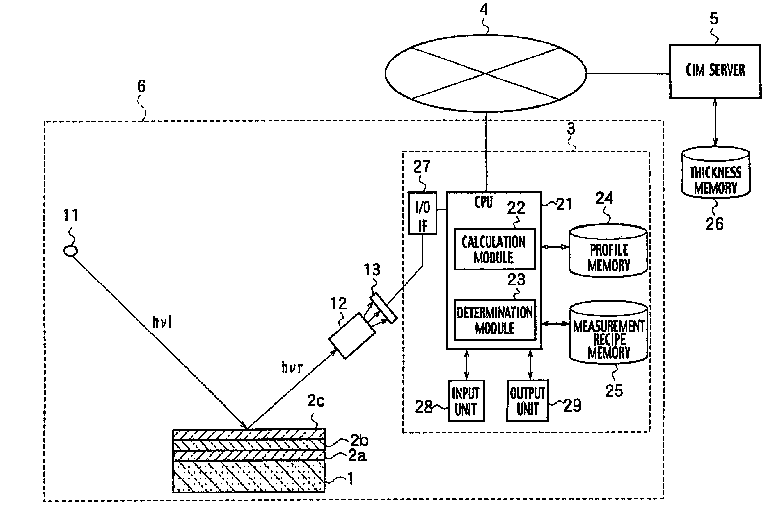
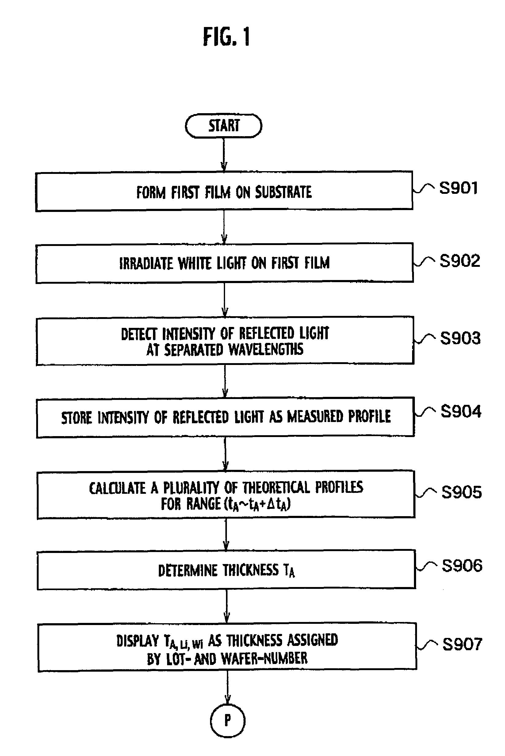
[0047]As shown in FIG. 5, a thickness monitoring system according to a first embodiment of the present invention encompasses a thickness-measuring tool 6 and a CIM server (measurement control server) 5. The thickness-measuring tool 6 is connected to the CIM server 5 through a communication network 4 such as local area network (LAN). Namely, the thickness monitoring system of the first embodiment is a control system configured to control in-line monitoring of various thin films by a single thickness-measuring tool 6 and the CIM server 5. Here, the various thin films may include silicon oxide (SiO2) films grown by thermal oxidation or deposited by chemical vapor deposition (CVD), sputtering, vacuum evaporation processes; phosphosilicate glass (PSG) films, boro-phosphate-silicate glass (BPSG) film, silicon nitride (Si3N4) film, and poly-silicon films deposited by CVD; and metallic films deposited by CVD, sputtering, or vacuum evaporation processes.
[0048]A thickness memory 26, which sto...
second embodiment
[0083]As shown in FIG. 14, a thickness monitoring system according to a second embodiment of the present invention encompasses a plurality of thickness-measuring tools 6a, 6b, 6c, . . . , a CIM server (measurement control server) 5, and a communication network 4 such as LAN to which the thickness-measuring tools 6a, 6b, 6c, . . . and the CIM server are connected. Namely, in the thickness monitoring system of the second embodiment, the single CIM server (measurement control server) 5 controls the thickness-measuring tools 6a, 6b, 6c, . . . . A first thickness-measuring tool 6a, a second thickness-measuring tool 6b, and a third thickness-measuring tool 6c, . . . execute respectively in-line thickness monitoring of miscellaneous thin film formation processes of various thin films, which may include SiO2 films grown by steam (wet) oxidation, grown by dry oxidation, deposited by CVD, deposited by sputtering, deposited by vacuum evaporation; PSG film, BPSG film, Si3N4 film, and poly-silic...
third embodiment
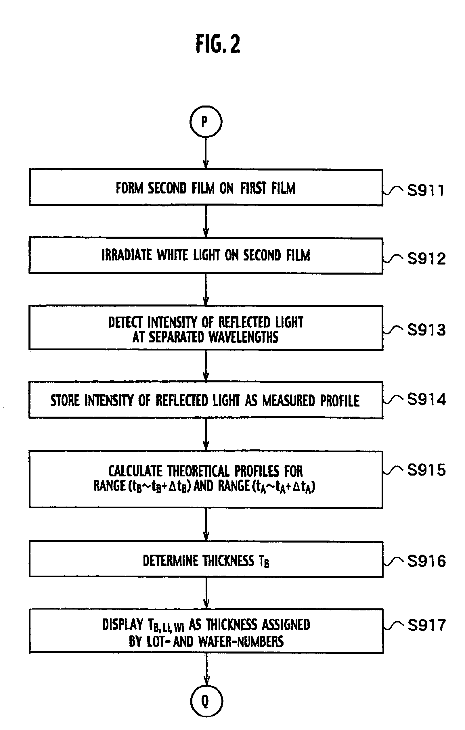
[0110]FIG. 23 is a data flow diagram describing operation of a thickness monitoring system according to a third embodiment of the present invention in a case executing in-line thickness monitoring of a three-layers structure. The thickness monitoring system according to the third embodiment corresponds to a thickness monitoring system that is a combination of the first and second embodiments, as shown in FIG. 23. Namely, in a thickness monitoring method according to the third embodiment (in-line monitoring), a thickness-measuring tool 6p acquires commonly a plurality of actual measured reflection spectrums of different layers of thin films, such as the reflection spectrums of the first film 2a and the second film 2b. These actual measured reflection spectrums are commonly processed by a common measuring-tool-side computer 3 of the first thickness-measuring tool 6p, and measurement values are arithmetically calculated for both of the first film 2a and the second film 2b. On the other...
PUM
 Abstract
Description
Claims
Application Information