Metal nanowire thin-films

a metal nanowire and thin film technology, applied in the direction of dielectric characteristics, liquid/solution decomposition chemical coating, conductors, etc., can solve the problems of limited transparency/conductivity trade-off between film and film, hard and brittle films, expensive vacuum deposition techniques, etc., to enhance the characteristics of nanowire films

Active Publication Date: 2011-07-07
TECH INNOVATION MOMENTUM FUND ISRAEL
View PDF5 Cites 42 Cited by
  • Summary
  • Abstract
  • Description
  • Claims
  • Application Information

AI Technical Summary

Benefits of technology

[0123]For some applications it may be necessary to embed the nanowire film in a solid matrix, with portions of the nanowires extending from the matrix to enable access to a conductive network. Such a matrix may provide protection to the nanowires from adverse factors such as corrosion and abrasion. The matrix may also offer mechanical properties to the conductive nanowire layer.
[0124]Additionally, performance-enhancing layers may be used to further enhance the...

Problems solved by technology

These films have a limited transparency/conductivity trade-off and are produced by expensive vacuum deposition techniques.
Such films are also hard and brittle and may therefore be unsuitable for flexible coatings such as plastic electronics.
A flexible alternative that has been considered is a film of a conducting polymer, but such films are much less conductive and more sensitive to radiation and chemical attack and would thus not be good candidates for ITO replacement.
However, such films could not exceed the performance of ITO films in terms of conductivity vs. visible light transmittance.
There are several problems in producing highly conductive, transparent carbon nanotube mesh films.
The limited solubility of the tubes makes it difficult to ...

Method used


Image

  • Metal nanowire thin-films
  • Metal nanowire thin-films
  • Metal nanowire thin-films

Examples


example 1

[0154]A 8.3% (w / w) cetyltrimethylammonium bromide (CTAB) solution was prepared by heating and stirring the CTAB / water mixture at 50?C for 5 minutes. To this solution, at 40?C, 500 μL of 25 mM HAuCl4 solution and 425 μL of 1.8 M freshly prepared sodium ascorbate solution were added and stirred together. Then, 250 μL of 100 mM AgNO3 solution were added while stirring. The final CTAB concentration in the nanowire growth solution was ˜7.5%. 30 seconds after the addition of the Ag solution, the stirring was discontinued and the solution was deposited on a substrate and let dry for 15-45 minutes at 35-40° C.

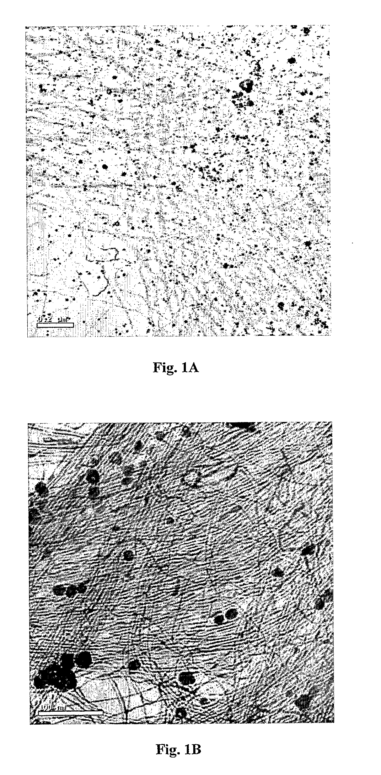
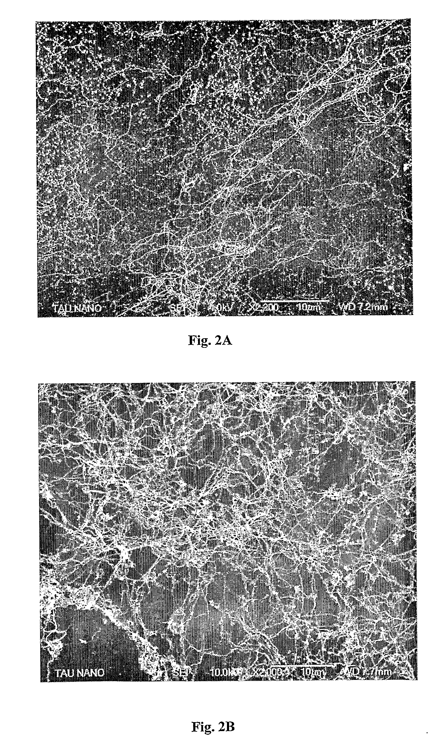
[0155]Transmission electron microscopy (TEM) and scanning electron microscopy (SEM) imaging revealed metal nanowire networks of varying wire densities and entanglement, depending on the exact solution and deposition conditions, uniformly spread over the substrates (FIGS. 1 and 2). The nanowires were typically 3-5 nm wide and many micrometers long and in this case composed of 85-90% gol...

example 2

[0160]A solution comprising surfactant cetyltrimethylammonium bromide (CTAB), chloroauric acid, as a gold precursor at a molar ratio of 1:200 relative to the CTAB concentration, and sodium ascorbate, at a molar ratio of 60:1 relative to the gold concentration, was prepared. The nanowire growth solutions had CTAB concentrations of 0.25 M and 0.6 M, significantly higher than the 0.1 M used by Murphy [1,2]. In addition, the growth solution contained a relatively high concentration of silver nitrate, twice the concentration of the Au(III) ions. When the four components were mixed together at 35?C the gold ions were reduced to the colorless Au(I) state, forming a [AuX2]−-CTA+ comply (X═Cl, Br) but further reduction to the metallic state required the addition of catalytic metal seed particles. Similarly, the silver ions formed an AgBr-CTAB complex.

[0161]As an alternative, a small amount of sodium borohydride dissolved in water (e.g., 0.001-0.0001%) was added to the precursor solution in o...

example 3

[0169]As recited above, in some experiments, prior to the addition of the reducing agent (e.g., sodium ascorbate) to the Au precursor solution, the silver solution was added to the Au precursor solution and only then the mild reducing agent e.g., sodium ascorbate was added. Under such conditions no metal reduction was induced. Subsequently, low concentration (e.g., 1 / 100 of that of the sodium ascorbate or lower) of a stronger reducing agent with respect to ascorbate was added to the solution. Such stronger reducing agent should have a reduction potential)(E0) of −0.5 V or more negative. Non-limiting examples are sodium borohydride, sodium cyanoborohydride and hydrazine. The addition of the strong reducing agent initiated metal reduction in this solution and subsequent metal deposition on the substrate.


PUM

PropertyMeasurementUnit
Fractionaaaaaaaaaa
Fractionaaaaaaaaaa
Timeaaaaaaaaaa

Abstract

A conductive nanowire film based on a high aspect-ratio metal is disclosed. The nanowire film is produced by inducing metal reduction in a concentrated surfactant solution containing metal precursor ions, a surfactant and a reducing agent. The metal nanostructures demonstrate utility in a great variety of applications.

Description

FIELD OF THE INVENTION[0001]This invention relates to the formation of metal nanowire thin-films.BACKGROUND OF THE INVENTION[0002]Applications of thin, transparent and electrically conducting films are numerous. The most attractive application is as a transparent electrode for low-cost photovoltaics and other opto-electronic applications. Light emitting devices often require such electrodes, in particular, large area displays. Currently, the existing technology uses conducting metal oxide films, primarily indium-tin oxide (ITO) and doped zinc oxide for these applications. These films have a limited transparency / conductivity trade-off and are produced by expensive vacuum deposition techniques. Such films are also hard and brittle and may therefore be unsuitable for flexible coatings such as plastic electronics. A flexible alternative that has been considered is a film of a conducting polymer, but such films are much less conductive and more sensitive to radiation and chemical attack ...

Claims


Application Information

Patent Timeline
IPC IPC(8): H01B5/00B05D5/12B05D3/06
CPCC23C18/14C23C18/166C23C18/1676C23C18/34C23C18/40C23C18/44H05K2203/125H05K3/105H05K3/182H05K2201/0257H05K2203/013H05K2203/1157C23C18/48Y10T428/24917H01B1/02C23C18/143C23C18/1667H01L29/786H05K1/0274H05K1/09H05K2201/0108H05K2201/026H05K2201/10121H05K2201/10128H05K2201/10166
Inventor MARKOVICH, GILAZULAI, DANIELKRICHEVSKI, OLGA
Owner TECH INNOVATION MOMENTUM FUND ISRAEL
Why Eureka
Try Eureka