

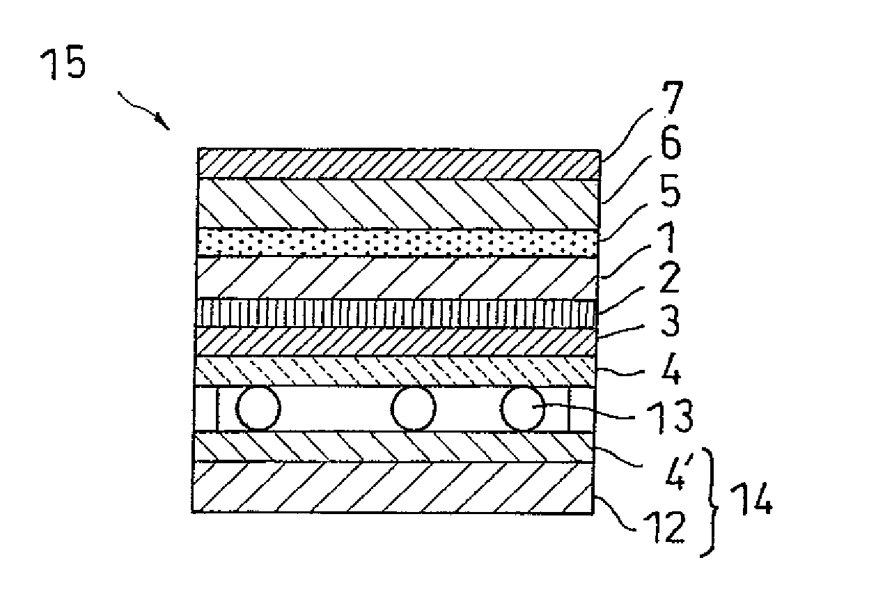
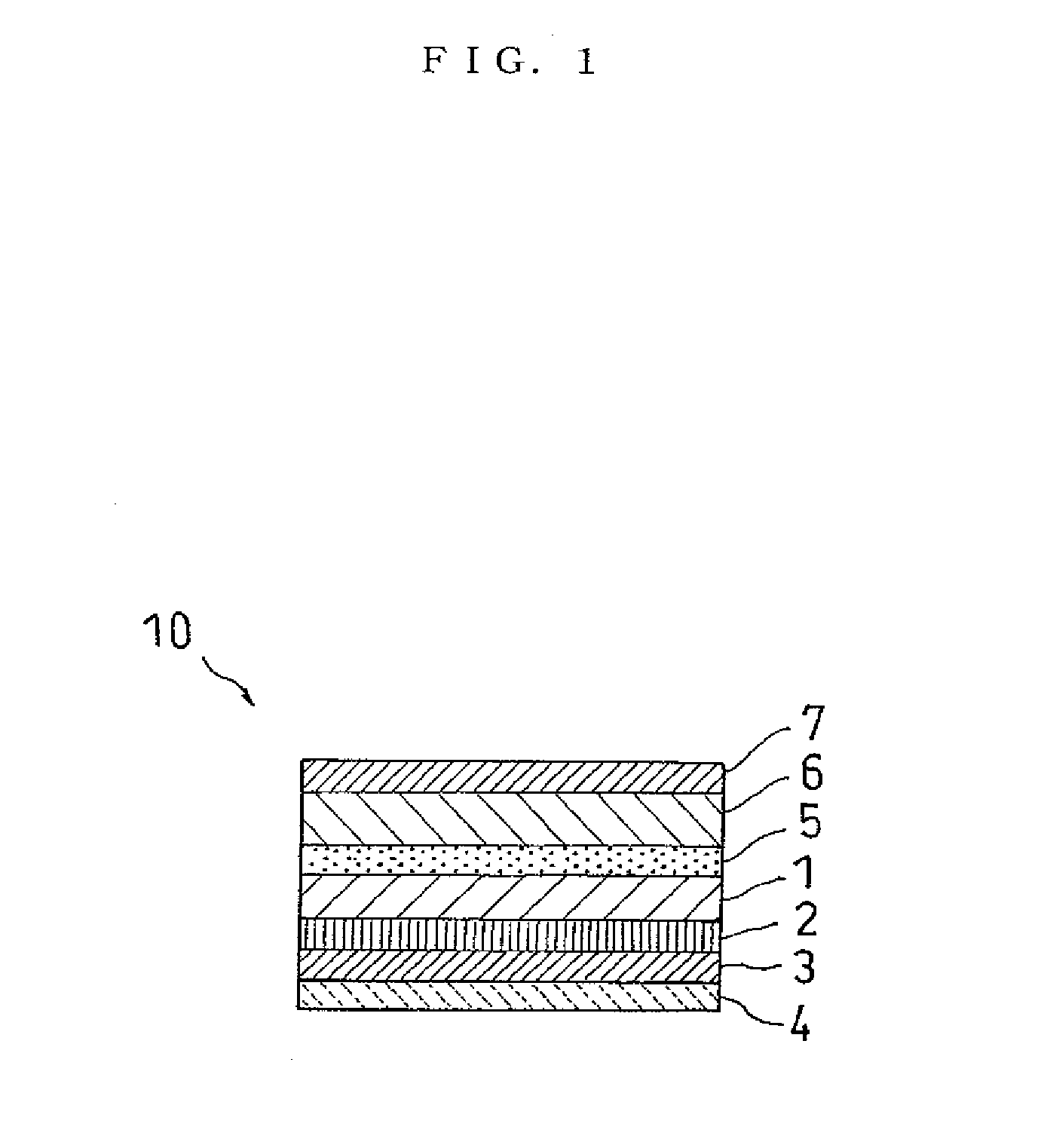
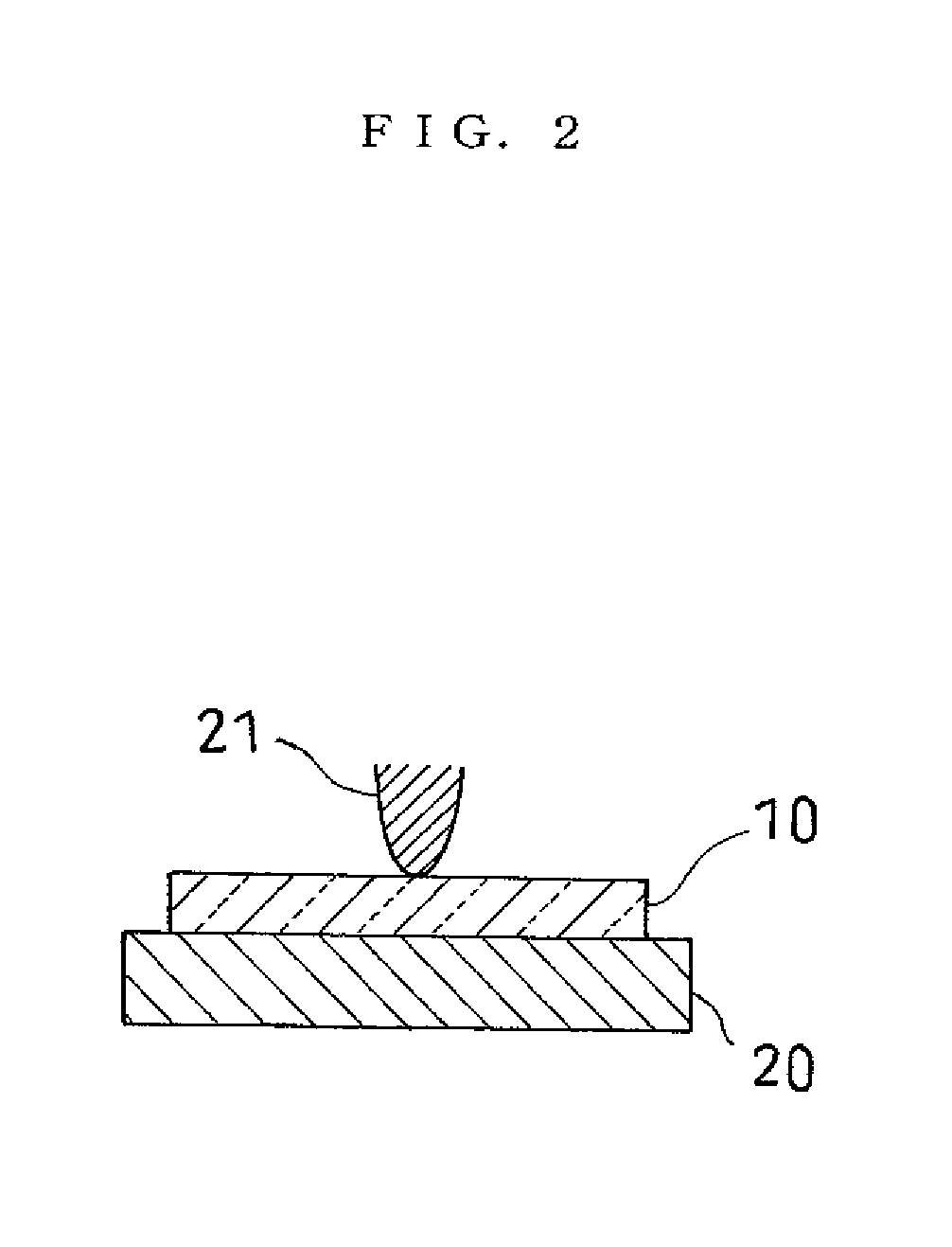
Transparent conductive multilayer body and touch panel having same
a multi-layer, touch-panel technology, applied in the direction of record information storage, natural mineral layered products, synthetic resin layered products, etc., can solve the problems of inability to reliably and reliably, change in the electrical resistance value on the surface of the transparent conductive layer, and inferior durability against input by the pen in the peripheral portions
- Summary
- Abstract
- Description
- Claims
- Application Information
AI Technical Summary
Benefits of technology
Problems solved by technology
Method used
Image

Examples
example 1
[0078] [Formation of Conductive Thin Film]
[0079] An SiOx film (relative index of refraction: 1.80; thickness: 15 nm) was formed on one surface of a film base made of a polyethylene terephthalate film (hereinafter referred to as PET film) having a thickness of 25 μm in accordance with a vacuum vapor deposition method.
[0080] Next, an SiO2 film (relative index of refraction: 1.46; thickness: 30 nm) was formed on the SiOx film in accordance with a vacuum vapor deposition method. Next, an ITO film (conductive thin film having a relative index of refraction of 2.00) having a thickness of 25 nm was formed on the SiO2 film in accordance with a reactive sputtering method using a sintered material having 95 wt % of indium oxide and 5 wt % of tin monoxide in an atmosphere of 80% argon gas and 20% oxygen gas under 4×10⁻³ Torr. In addition, the ITO film was crystallized through heat treatment at 150° C. for one hour.
[0081] [Formation of Hard Coat Layer]
[0082] 5 parts of hydroxycyclohexyl pheny...
example 2
[0086] In the present example, a transparent conductive multilayer body was fabricated in the same manner as in Example 1, except that the relative index of refraction of the SiOx film was 1.75.
example 3
[0087] In the present example, a transparent conductive multilayer body was fabricated in the same manner as in Example 1, except that the relative index of refraction of the SiOx film was 1.70.
PUM
| Property | Measurement | Unit |
|---|---|---|
| thickness | aaaaa | aaaaa |
| thickness | aaaaa | aaaaa |
| thickness | aaaaa | aaaaa |
Abstract
Description
Claims
Application Information