Printed circuit board design system

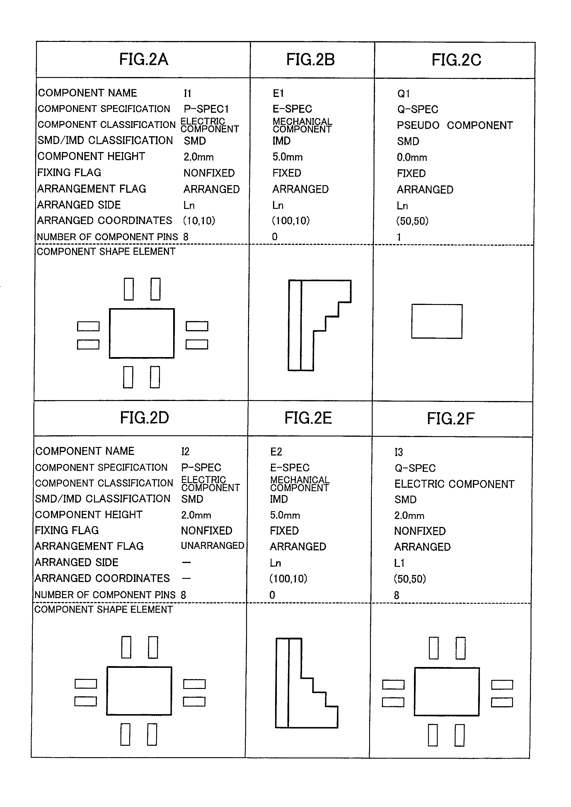
a technology of printed circuit boards and design systems, applied in the field of printed circuit board design systems, can solve the problems of reducing the size of printed circuit boards, requiring mounting design man-hours, and unable to recognize the fixed/nonfixed state of components i4-i6 by 3d models

Inactive Publication Date: 2002-04-18
FUJITSU LTD
View PDF0 Cites 24 Cited by
  • Summary
  • Abstract
  • Description
  • Claims
  • Application Information

AI Technical Summary

Problems solved by technology

With this demand, its printed circuit board has been downsized / complicated, so that accuracy of outer dimensions, which is required for removing an interference with a cabinet, and besides reduction of mounting design man-hours have been demanded.
However, fixed / nonfixed states of the components I4-I6 can not be recognized by the 3D models.
In 3D modeling by such a prior art PCB-CAD system, there is a possibility that man-hours increase and manual mistakes occur as follows:
{circle over (4)} The mechanical component or the like was modeled by the maximum rectangular shape, so that the inspection of the cabinet interference was inaccurate, leading to an occurrence of interference which does not inherently exist.

Method used


Image

  • Printed circuit board design system
  • Printed circuit board design system
  • Printed circuit board design system

Examples


Embodiment Construction

[0063] The present invention will be described referring to the attached drawings in order to specify the invention in more detail.

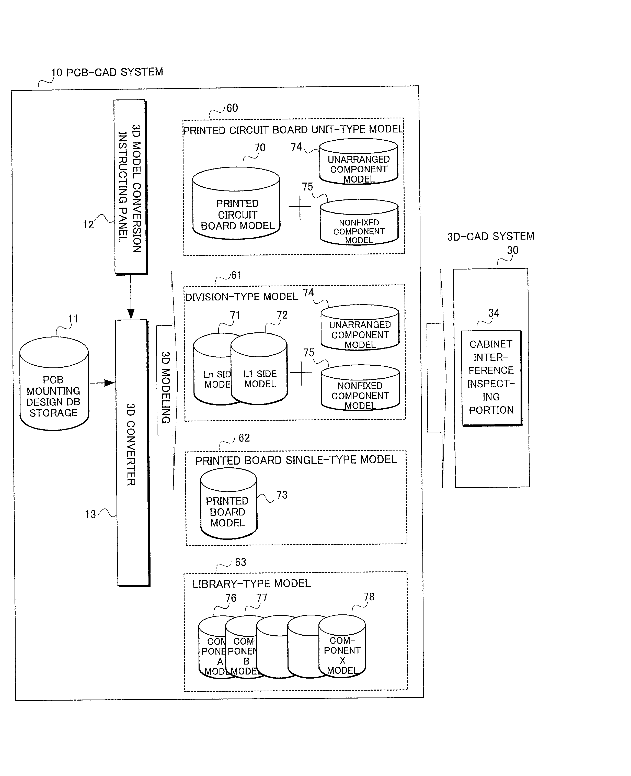
[0064] FIG. 1 shows an embodiment of a PCB-CAD system 10 according to the present invention. This CAD system 10 is composed of a PCB mounting design DB (database) storage 11, a 3D converter 13 for inputting information of a PCB mounting design DB from the DB storage 11 and for converting a printed circuit board into a 3D model, and a 3D model conversion instructing panel 12 for instructing the 3D converter of the condition of the conversion.

[0065] Also, FIG. 1 shows 3D model examples converted by the 3D converter, including a printed circuit board unit-type model 60, a division-type model 61, a printed board single-type model 62, and a library-type model 63.

[0066] The unit-type model 60 is composed of a printed circuit board model 70, an unarranged component model 74, and a nonfixed component model 75. The division-type model 61 is composed of an Ln side...


PUM


Abstract

A printed circuit board design system performs, with a 3D-CAD system, a mounting design including a cabinet. In order to prepare, without mistakes in less man-hours, an accurate 3D model of a printed circuit board provided to the 3D-CAD system, a converter converts the printed circuit board into a unit-type model, a division-type model, a single-type model, and a library-type model composed of one or more models based on attributes preliminarily added to a mounting component stored in a mounting design DB storage.

Description

[0001] 1. Field of the Invention[0002] The present invention relates to a printed circuit board design system, and in particular to a printed circuit board design system for performing, with a three-dimensional (3D)-CAD system, a mounting design including a cabinet.[0003] 2. Description of the Related Art[0004] In recent electronic equipment such as mobile terminal equipment, not only the downsizing / complication of its shape but also the reduction of its TTM (Time To Market) has been demanded. With this demand, its printed circuit board has been downsized / complicated, so that accuracy of outer dimensions, which is required for removing an interference with a cabinet, and besides reduction of mounting design man-hours have been demanded.[0005] A prior art printed circuit board design system completes the arrangement of mounting components (parts) on a printed board, and then generates a 3D (three-dimensional) model (data) of a printed circuit board unit. Based on this model, a 3D-CAD...

Claims


Application Information

Patent Timeline
Patent Type & Authority Applications(United States)
IPC IPC(8): H05K13/08
CPCH05K13/08H05K3/0005G06F30/39G06F30/00G06F2115/12
Inventor MATSUSHITA, HIDEHARUNAKAYAMA, MASAYUKI
Owner FUJITSU LTD
Why Eureka
Try Eureka