Method of manufacturing panel switch and panel switch

A panel switch and manufacturing method technology, applied to the panel switch manufacturing, panel switch manufacturing method and the field of panel switches, can solve the problems of waste of mold correction costs and production time, increased man-hours, decreased operability, etc., to achieve finished products The effect of increasing the efficiency, reducing the area and eliminating the position deviation

Active Publication Date: 2008-12-31
MITSUMI ELECTRIC CO LTD
View PDF1 Cites 26 Cited by
  • Summary
  • Abstract
  • Description
  • Claims
  • Application Information

AI Technical Summary

Problems solved by technology

[0015] However, the above-mentioned existing panel switch 51 needs to punch out a plurality of insulating film sheets 54a, 54a from the insulating film 24 by using a mold, and lay them sequentially on the jig 56, so there is a significant increase in man-hours. increase, and the operability decreases, resulting in an increase in cost
In addition, when the shape of the insulating film sheet 54a is changed, the mold must be corrected according to the change, and the cost and production time for mold correction are wasted, which becomes a cause of cost increase.

Method used


Image

  • Method of manufacturing panel switch and panel switch
  • Method of manufacturing panel switch and panel switch
  • Method of manufacturing panel switch and panel switch

Examples


Embodiment

[0073] Hereinafter, the structure of the panel switch manufactured by the manufacturing method of this invention is given and demonstrated with preferable Example together with the manufacturing method. This embodiment is suitable for a panel switch shipped as a product in a state where a plurality of insulating film sheets are mounted on a wiring board or a spacer as a base member.

no. 1 approach

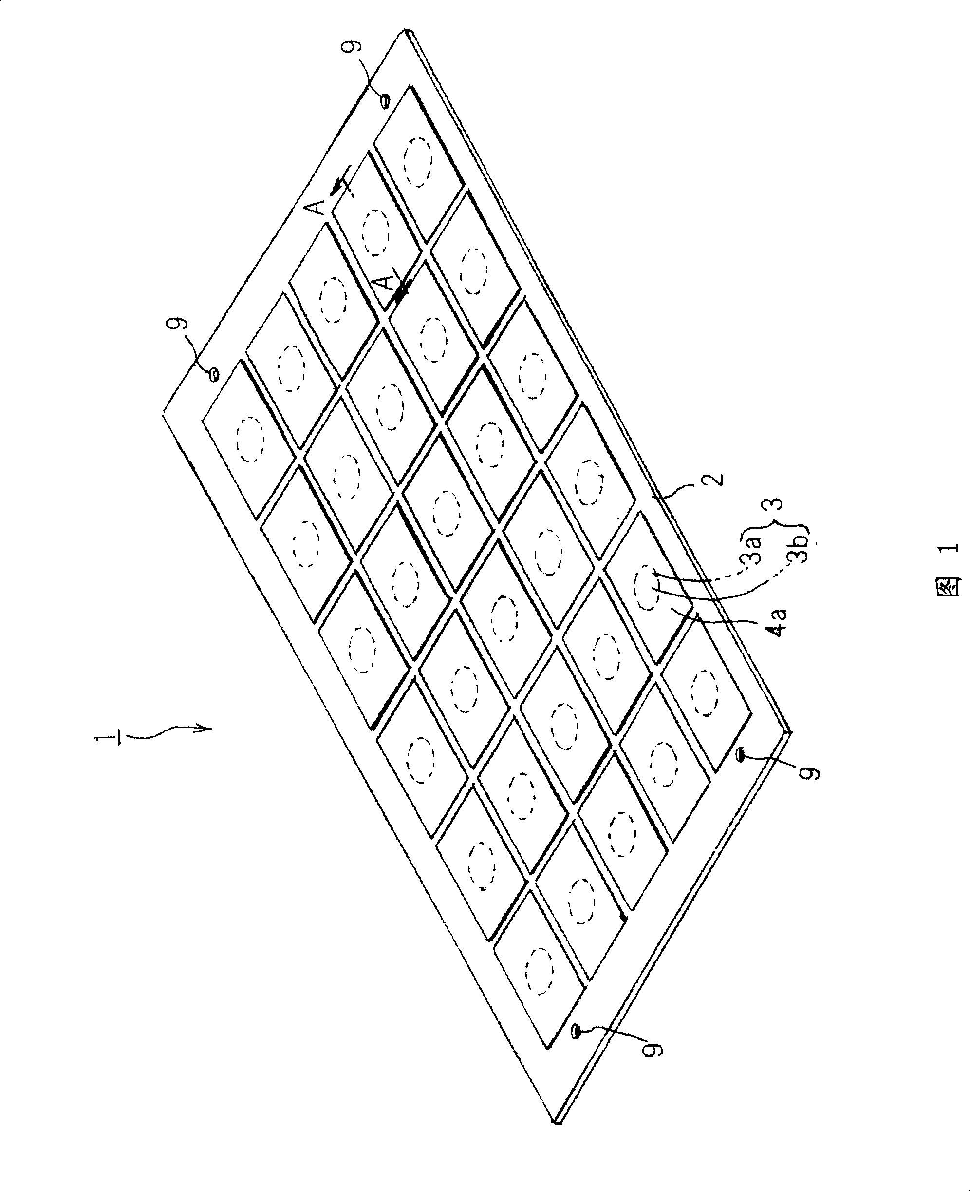
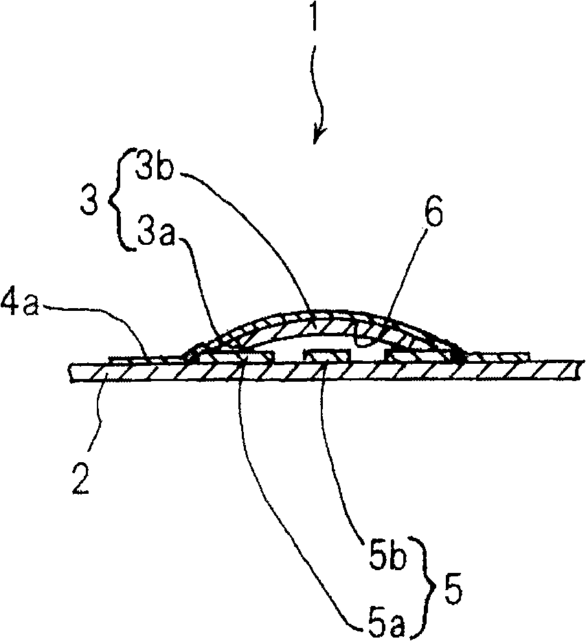
[0075] 1 is a perspective view of a panel switch manufactured by the manufacturing method of the first embodiment, figure 2 It is an enlarged cross-sectional view taken along line A-A of FIG. 1 . Figure 1 and figure 2 The panel switch 1 shown uses a wiring board 2 as a base member.

[0076] In Figure 1 and figure 2 Among them, the panel switch 1 includes: a wiring board (base member) 2 having a plurality of fixed contacts 5; a plurality of, for example, 30 movable contacts 3, 3... disposed on the wiring board 2; and A plurality of insulating film sheets 4a, 4a... are mounted on the wiring board 2 to cover the movable contacts 3, 3..., respectively.

[0077] Such as figure 2 As shown, on the above-mentioned wiring board 2, fixed contacts 5 are respectively provided by printing or the like on the surface of the sheet-shaped insulating film and at a plurality of places where the switch section is formed. Each fixed contact 5 includes: an outer electrode 5a formed in a su...

no. 2 approach

[0100] Figure 9 It is a manufacturing process drawing showing the second embodiment of the present invention, Fig. 10 and Figure 11 It is a structural diagram and a sectional view of the panel switch 21 manufactured by the manufacturing method of 2nd Embodiment. In the manufacturing method of the second embodiment, the movable contact superposition step (E) is added to the manufacturing steps (A) to (D) of the first embodiment, and the other steps are substantially the same as the manufacturing steps of the first embodiment.

[0101] Moreover, the panel switch 21 manufactured through the manufacturing process of the second embodiment is also the same as the first embodiment. The movable contacts 3, 3... are mounted on the adhesive layer 6 of the above-mentioned insulating film 4. The insulating films 4 of the movable contacts 3, 3... are different in that they are laminated in two layers, and the other structures are the same. Therefore, the same symbols are assigned to the...


PUM


Abstract

The invention provides a method for manufacturing a panel switch with reduced man hour, improved operability and lowered cost. The panel switch and a method of manufacturing the same are provided. The panel switch includes insulating films and a base layer having a stationary contact. Each insulating film includes an adhesive layer, and an apex portion of a moving contact adhered to the adhesive layer. The insulating films are aligned and adhered on top of each other and the adhered insulating films are aligned and adhered to the base layer such that the locations of the moving contacts of the respective insulating films align with the stationary contact of the base layer. The method includes applying an adhesive layer to an insulating film; adhering a moving contact onto the adhesive layer; aligning the moving contact with a stationary contact of a base member and adhering the insulating film to the base member; and cutting and removing an excess portion from the insulating film with a laser.

Description

technical field [0001] The present invention relates to a method of manufacturing a panel switch and a panel switch, and more particularly to a method of manufacturing a panel switch and a panel switch used for thin operation panels of various electronic devices such as input operation units of mobile phones and computer-related equipment. Background technique [0002] In recent years, input and operation parts for inputting and outputting information to communication equipment or computer-related equipment have been required to be thinner and cheaper, and the use of sheet-shaped panel switches has become popular (for example, refer to Patent Document 1: Japanese Patent Laid-Open 2003-100165 Bulletin). [0003] Fig. 15 is a perspective view of a conventional panel switch, Figure 16 It is an enlarged sectional view taken along line C-C in FIG. 15 . In the two figures, the panel switch 51 has: a wiring board 52; a plurality of, for example, 30 movable contacts 53, 53... disp...

Claims


Application Information

Patent Timeline
Patent Type & Authority Applications(China)
IPC IPC(8): H01H13/88H01H13/702B23K26/00B23K26/38H01H11/00H01H13/48
CPCH01H13/48H01H13/88H01H2205/026H01H2215/036H01H2229/02H01H2229/034Y10T29/49155Y10T156/108Y10T29/49117Y10T29/49105Y10T29/49204
Inventor 菊池秀武寺下俊彦井上刚河村乔
Owner MITSUMI ELECTRIC CO LTD
Why Eureka
Try Eureka