Wiring structure in semiconductor device and method for forming the same

a technology of wiring structure and semiconductor device, which is applied in the direction of semiconductor device, semiconductor device details, electrical apparatus, etc., can solve the problems of inhibiting the higher performance of a semiconductor device, high stress, and low polishing rate during chemical/mechanical polishing, so as to achieve less easily oxidizable, less easily oxidizable, and effective prevention of cracking of refractory metal layers

Inactive Publication Date: 2002-05-23
SONY CORP
View PDF0 Cites 11 Cited by
  • Summary
  • Abstract
  • Description
  • Claims
  • Application Information

AI Technical Summary

Benefits of technology

[0017] Further, it is a second object of the present invention to provide a wiring structure in a semiconductor device, which, in addition to achieving the above first object, can prevent a refractory metal layer from undergoing cracking and is free from the inhibition of growth of the refractory metal layer, and a method for forming the wiring structure.
[0018] It is further a third object of the present invention to provide a wiring structure in a semiconductor device, which, in addition to achieving the above first object, can reliably prevent the adverse influence caused by the gas released from an insulating layer composed of a low dielectric constant material and is free from the inhibition of growth of the refractory metal layer, and a method for forming the wiring structure.
[0027] In the method for forming a wiring structure in a semiconductor device in the present invention, for achieving the above third object, preferably, the step (c) comprises a step of forming the thin layer of a metal or a metal compound on the barrier metal layer by an ionized sputtering method or a long throw sputtering method, and the above step (d) comprises a step of forming a refractory metal layer on the thin layer by a chemical vapor deposition method to fill the inside(s) of the opening portion and / or the trench portion with the refractory metal layer. This method for forming a wiring structure in a semiconductor device, provided by the present invention, will be referred to as a method for forming a wiring structure in a semiconductor device according to the second aspect of the present invention for the convenience. In this case, the temperature for heating the insulating layer during the formation of the refractory metal layer is required to be lower than the pyrolysis initiation temperature of the low dielectric constant material constituting the insulating layer. The above ionized sputtering method refers to a sputtering method in which particles sputtered from a target are passed through a plasma having an electron density of 10.sup.10 to 10.sup.12 cm.sup.-3 and the sputtered particles ionized by their collision with the plasma are directed perpendicularly to the insulating layer with a bias voltage applied to the substratum, which method can improve the coverage on the opening portion and / or the trench portion. The above long throw sputtering method refers to a sputtering method in which the distance between the target and the substratum is increased to intensify the perpendicular directionality of the sputtered particles to the insulating layer, which method can also improve the coverage on the opening portion and / or the trench portion.
[0042] In the present invention, the thin layer is composed of a metal or a metal compound which is less easily oxidizable than a material constituting the barrier metal layer, the thin layer corresponding to an underlayer for forming the refractory metal layer is less easily oxidizable, and there can be therefore avoided the problem that it is difficult to form the refractory metal layer.
[0043] In the wiring structure in a semiconductor device or the method for forming the wiring structure according to the first aspect of the present invention, the refractory metal layer having a tensile stress is formed on the thin layer having a compression stress, and the tensile stress of the refractory metal layer is therefore offset, so that the cracking of the refractory metal layer can be effectively prevented.
[0044] Further, in the wiring structure in a semiconductor device or the method for forming the wiring structure according to the second aspect of the present invention, the thin layer of a metal or a metal compound is formed on the barrier metal layer by the ionized sputtering method or the long throw sputtering method in which the directionality of sputtered particles are intensified, so that the coverage of the thin layer in the bottom of the opening portion and / or the trench portion can be improved. Further, for example, if a bias is applied to the substratum, the thin layer deposited in the bottom of the opening portion and / or the trench portion is re-sputtered, and as a result, the coverage of the thin layer on the inner wall surface(s) of the opening portion and / or the trench portion can be improved. Moreover, the thin layer is composed of a material which is less easily oxidizable than a material constituting the barrier metal layer. Therefore, not only the oxidation of the barrier metal layer can be prevented when the refractory metal layer is formed on the thin layer by a CVD method, but also the thin layer works as a barrier against gas released from the low dielectric constant material, and the process gases which the CVD method uses cannot be inhibited from entering the opening portion and / or the trench portion formed in the insulating layer composed of the low dielectric constant material. Therefore, the process gases are easily adsorbed on, and dissociated from, the thin layer, so that the opening portion and / or the trench portion can be reliably filled with the refractory metal layer. Further, if the thin layer is composed of the same refractory metal as the refractory metal which is to form the refractory metal layer to be formed on the thin layer, for example, if the thin layer is composed of tungsten, crystal nuclei of tungsten are easily formed on the thin layer, and the opening portion and / or the trench portion can be more reliably filled with the refractory metal layer. The above thin layer can therefore constitute an underlayer for forming the refractory metal layer according to a CVD method.

Problems solved by technology

With an increase in the integration degree of a semiconductor device, the design rule of a wiring of a semiconductor device keeps on becoming finer, and a signal delay caused by an increase in a capacitance between wirings is a serious problem which inhibits the higher performance of a semiconductor device.
However, the barrier metal layer composed of tantalum nitride has problems that it has a high stress and that it shows a low polishing rate during its chemical / mechanical polishing.
The reason therefor is that the tungsten layer formed by the blanket tungsten CVD method has poor adhesion to the insulating layer although it is excellent in step coverage.
However, when poly(aryl ether) of the following formula is used as a low dielectric constant material, and when the forming temperature is set at 420 to 470.degree. C., there occurs a phenomenon that the inside of the opening portion can no longer reliably filled with a tungsten layer.
That is, a failure in filling a tungsten layer in the opening portion takes place.
Process gases used in the blanket tungsten CVD method, such as WF.sub.6, SiH.sub.4 and H.sub.2, are prevented from entering an opening portion and / or a trench portion formed in the insulating layer, so that it is difficult to form a tungsten layer inside the opening portion and / or the trench portion, and the opening portion and / or the trench portion can no longer reliably filled with the tungsten layer.
As a result, a phenomenon that the tungsten layer undergoes cracking takes place, and the reliability of the wiring structure decreases.
Further, the barrier metal layer composed of TiN is liable to be oxidized.
When the barrier metal layer surface is oxidized, it is difficult to grow crystal nuclei of tungsten when tungsten is grown on the barrier metal layer by the blanket tungsten CVD method, and the crystal growth of the tungsten layer is inhibited.
Since, however, the above method involves a problem that the diameter of the opening portion decreases since the side-wall of an insulating material is formed on the inner wall surface of the opening portion or has a difficulty in that it is required to use SiN having a high relative dielectric constant, the above method cannot be said to be a satisfactory solution means when a low dielectric constant material is used for the insulating layer.

Method used


Image

  • Wiring structure in semiconductor device and method for forming the same
  • Wiring structure in semiconductor device and method for forming the same
  • Wiring structure in semiconductor device and method for forming the same

Examples


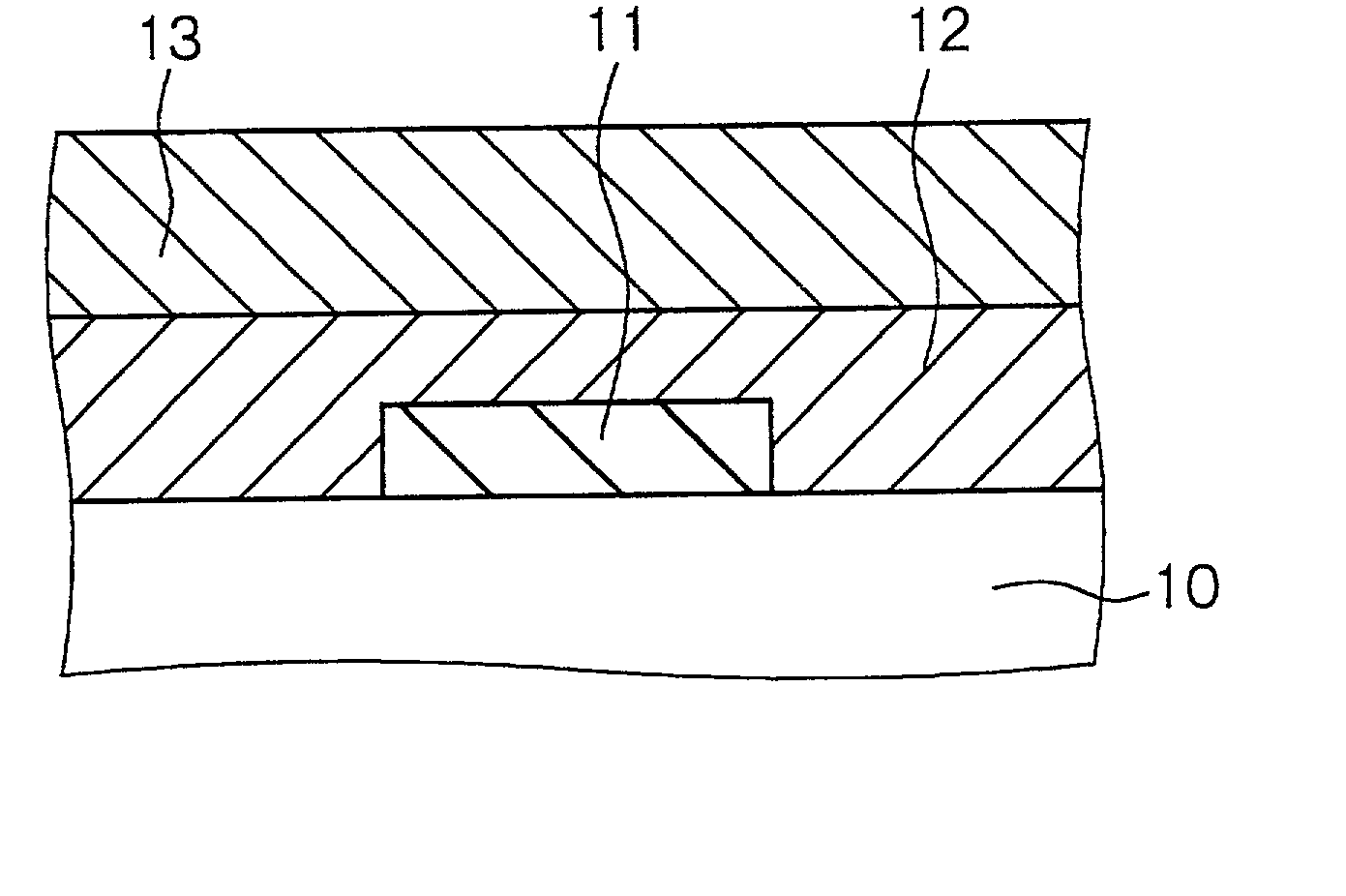
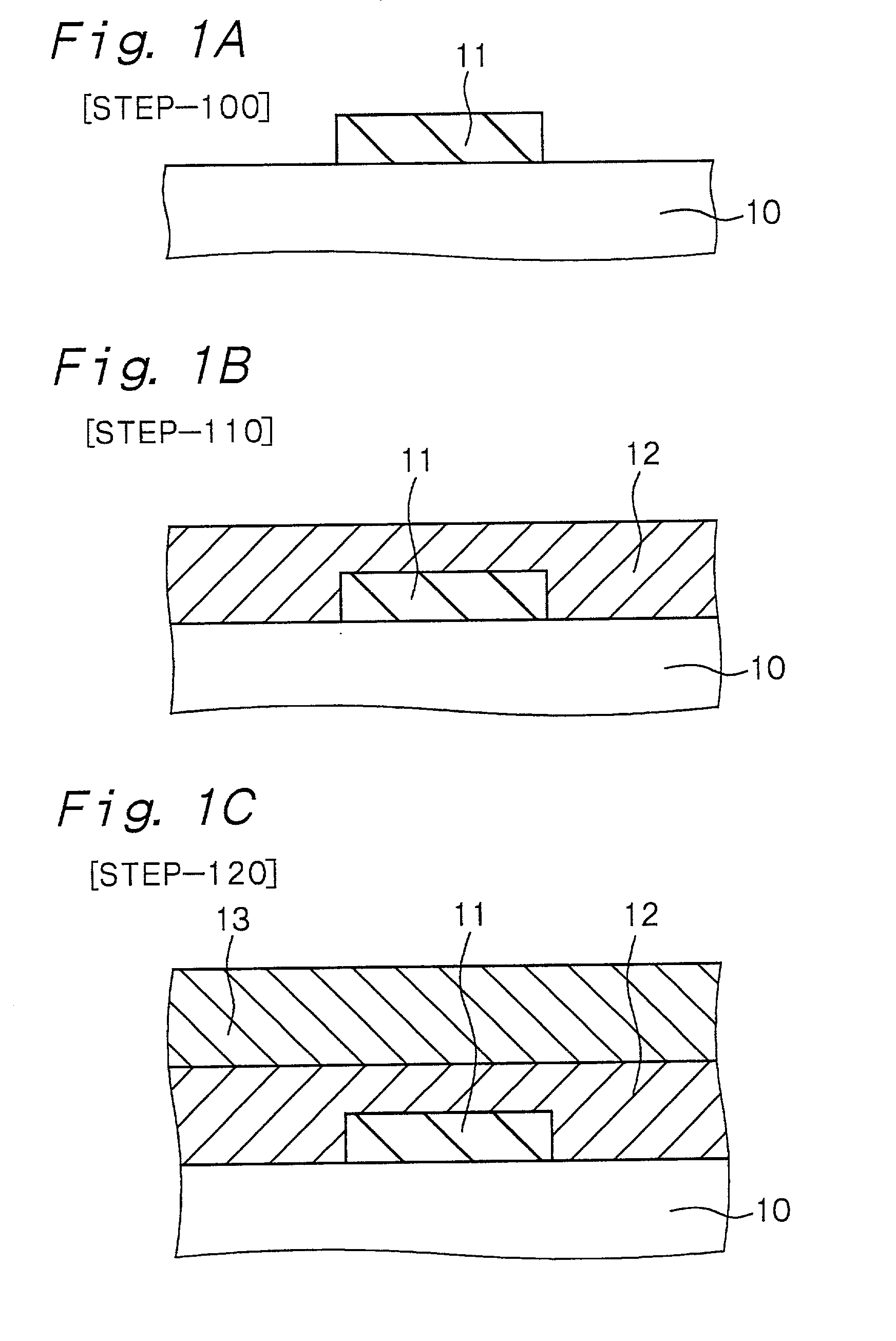
example 2

[0079] Example 2 is also concerned with the wiring structure in a semiconductor device according to the first and second aspects of the present invention. In Example 2, a thin layer composed of tungsten nitride (WN.sub.x) is formed by a long throw sputtering method. Further, an insulating layer is formed on a lower insulating layer, a trench portion is formed in the insulating layer, and a trench wiring is formed by filling the trench portion with a refractory metal layer. Like Example 1, poly(aryl ether) is used as a low dielectric constant material for constituting the insulating layer. Further, a barrier metal layer is composed of TiN, and the refractory metal layer composed of tungsten is formed by a CVD method. The wiring structure in a semiconductor device and the method for forming the wiring structure in Example 2 will be explained with reference to FIGS. 4A, 4B and 4C showing schematic cross-sectional views of the insulating layer, etc., hereinafter.

[0080] [Step-200]

[0081] ...


PUM

PropertyMeasurementUnit
dielectric constantaaaaaaaaaa
relative dielectric constantaaaaaaaaaa

Abstract

A method for forming a wiring structure in a semiconductor device, comprising the steps of: (a) forming an insulating layer of a low dielectric constant material having a relative dielectric constant of 3.5 or less and a pyrolysis initiation temperature of 400° C. or lower on a substratum and then forming an opening portion and / or a trench portion in the insulating layer, (b) forming a barrier metal layer on the insulating layer including an inside of the opening portion and / or the trench portion, (c) forming a thin layer on the barrier metal layer, and (d) forming a refractory metal layer on the thin layer to fill the inside of the opening portion and / or trench portion with the refractory metal layer, the thin layer being composed of a metal or a metal compound which is less easily oxidizable than a material constituting the barrier metal layer.

Description

BACKGROUND OF THE INVENTION AND RELATED ART STATEMENT[0001] The present invention relates to a wiring structure in a semiconductor device and a method for forming the wiring structure, and more specifically, it relates to a wiring structure in a semiconductor device, which wiring structure includes contacting holes such as a contact hole, a via hole and a through hole or a trench wiring, and a method for forming the wiring structure.[0002] A semiconductor device has a number of contact holes, through holes or via holes (these will be also generically referred to as "contacting holes" hereinafter). Generally, a contacting hole is formed by forming an insulating layer on an impurity-including region, various electrodes or a lower wiring layer (these will be also generically referred to as "lower conductive layer" hereinafter) formed in or on a semiconductor substrate, or forming an insulating layer on various electrodes or the lower wiring layer formed on a lower insulating layer; for...

Claims


Application Information

Patent Timeline
Patent Type & Authority Applications(United States)
IPC IPC(8): H01L21/28H01L21/768H01L23/522H01L23/532
CPCH01L23/5226H01L23/5329H01L23/53295H01L2924/0002H01L2924/00
Inventor MIYAMOTO, TAKAAKI
Owner SONY CORP
Why Eureka
Try Eureka