Display panel filter for connection to a display panel

a technology for filtering and display panels, applied in the direction of identification means, television systems, instruments, etc., can solve the problems of electromagnetic interference (emi) emissions, the depth dimension of display requires a significant amount, and new problems have arisen

Inactive Publication Date: 2002-06-20
WOODRUFF DANIEL P +1
View PDF11 Cites 17 Cited by
  • Summary
  • Abstract
  • Description
  • Claims
  • Application Information

AI Technical Summary

Benefits of technology

[0008] The preferred embodiment of the shielding film comprises one or more layers of a conductive material and one or more alternating layers of a dielectric. The conductive material may include various conductive metals or other materials such as silver, copper, gold and indium tin oxide, among others, although silver metal is preferred. The dielectric may include various materials such as niobium pentoxide, titanium dioxide and tin oxide, among others, although niobium pentoxide is preferred. Additionally, a thin protective layer is provided between adjacent conductive / dielectric layers to eliminate or limit undesirable oxidation or other deterioration of the conductive layer during formation of the film or otherwise. Such a protective layer is desirable when the conductive layer is subject to oxidation or other deterioration and / or the manufacturing conditions result in the film being exposed to high temperatures. Such conditions exist when the film is manufactured using sputtering or various other thin film deposition techniques, particularly for multiple layer films of two or more conductive material layers. In some cases, the protective layer is comprised of two or more layers of different materials.
[0014] Another object of the present invention is to provide a plasma display panel filter which provides anti-reflective, EMI shielding, contrast enhancement and infrared shielding capabilities and which also complies with consumer safety requirements.
[0018] A still further object of the present invention is to provide a plasma display panel fiter with an electrically conductive material around the edge of the filter to prevent environmental degradation of the EMI shielding layer and to maximize the EMI shielding efficiency of such layer.
[0019] A still further object of the present invention is to provide a plasma display panel as described above which includes a layer to prevent or minimize possible reactions between the lamination adhesive and the shielding film and / or to improve compatibility with the adhesive and promote the adhesive strength.

Problems solved by technology

First, a CRT display requires a significant depth dimension relative to the size of its display screen to accommodate a generally funnel shaped rearward portion for generation and deflection of the electron beam.
Second, most CRT screens are curved.
Although plasma display panels provide significant advantages and improvements by facilitating relatively large visual displays with a reduced panel depth and by otherwise facilitating the use of displays in environments with space restrictions which preclude the use of conventional CRT displays, new problems have arisen.
These problems relate to the quality of the visual display, increased infrared (IR) and electromagnetic interference (EMI) emissions, low contrast ratio and consumer safety issues.
This adversely affects the quality of the display.
Further, operation of the plasma display panel produces or has the potential of producing infrared (IR) emissions which are capable in some cases of interfering with a remote control of the panel or other devices utilizing infrared signaling.
Still further, operation of the plasma display panel results in the generation and emission of electromagnetic interference (EMI).
Accordingly, many plasma panel displays fail to meet governmental TCO and FCC requirements for EMI emissions and the stricter standards for various military, aircraft and other uses.
The above problems necessary limit the applicability and desirability of using plasma display panels.

Method used


Image

  • Display panel filter for connection to a display panel
  • Display panel filter for connection to a display panel
  • Display panel filter for connection to a display panel

Examples


Embodiment Construction

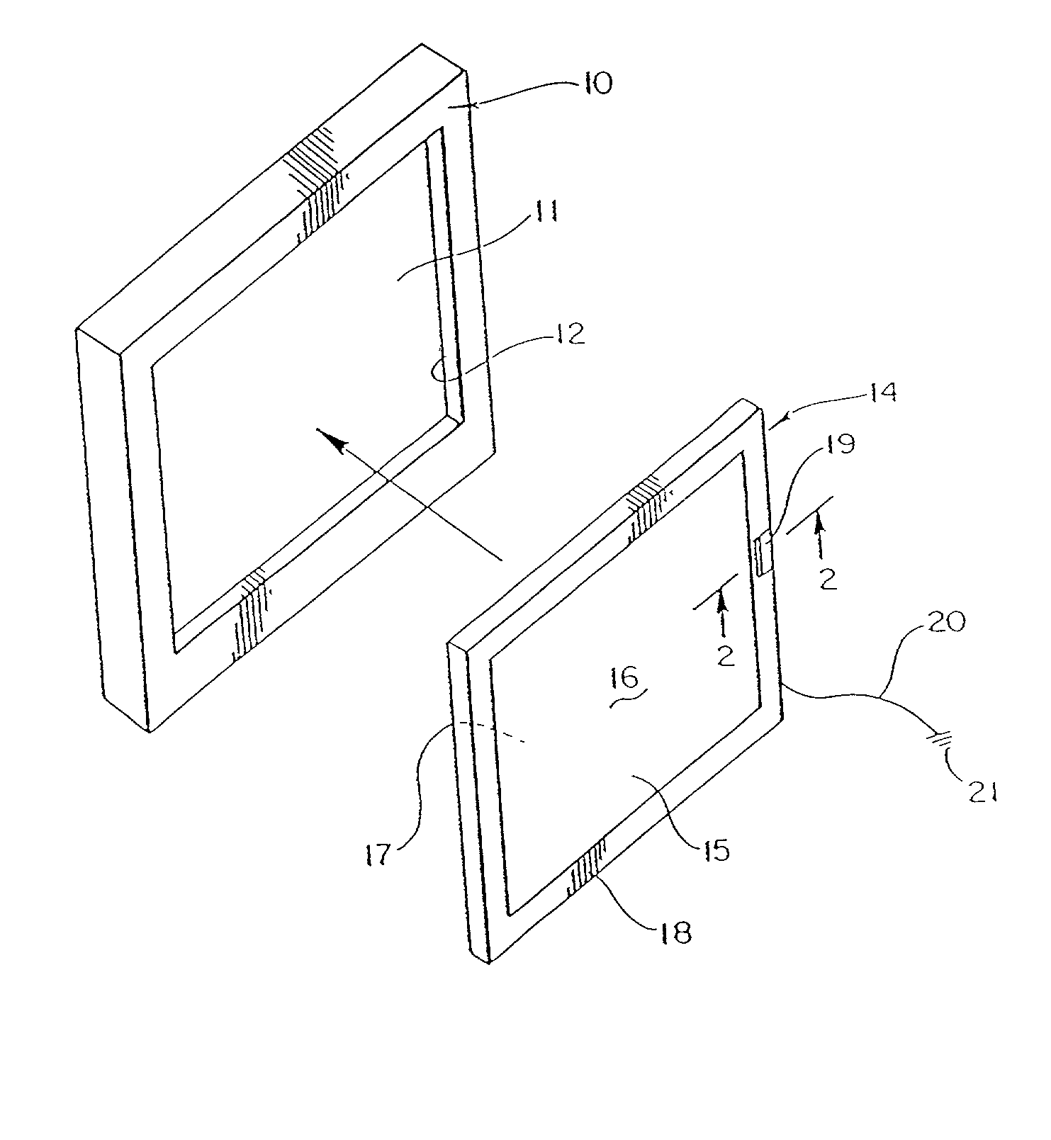
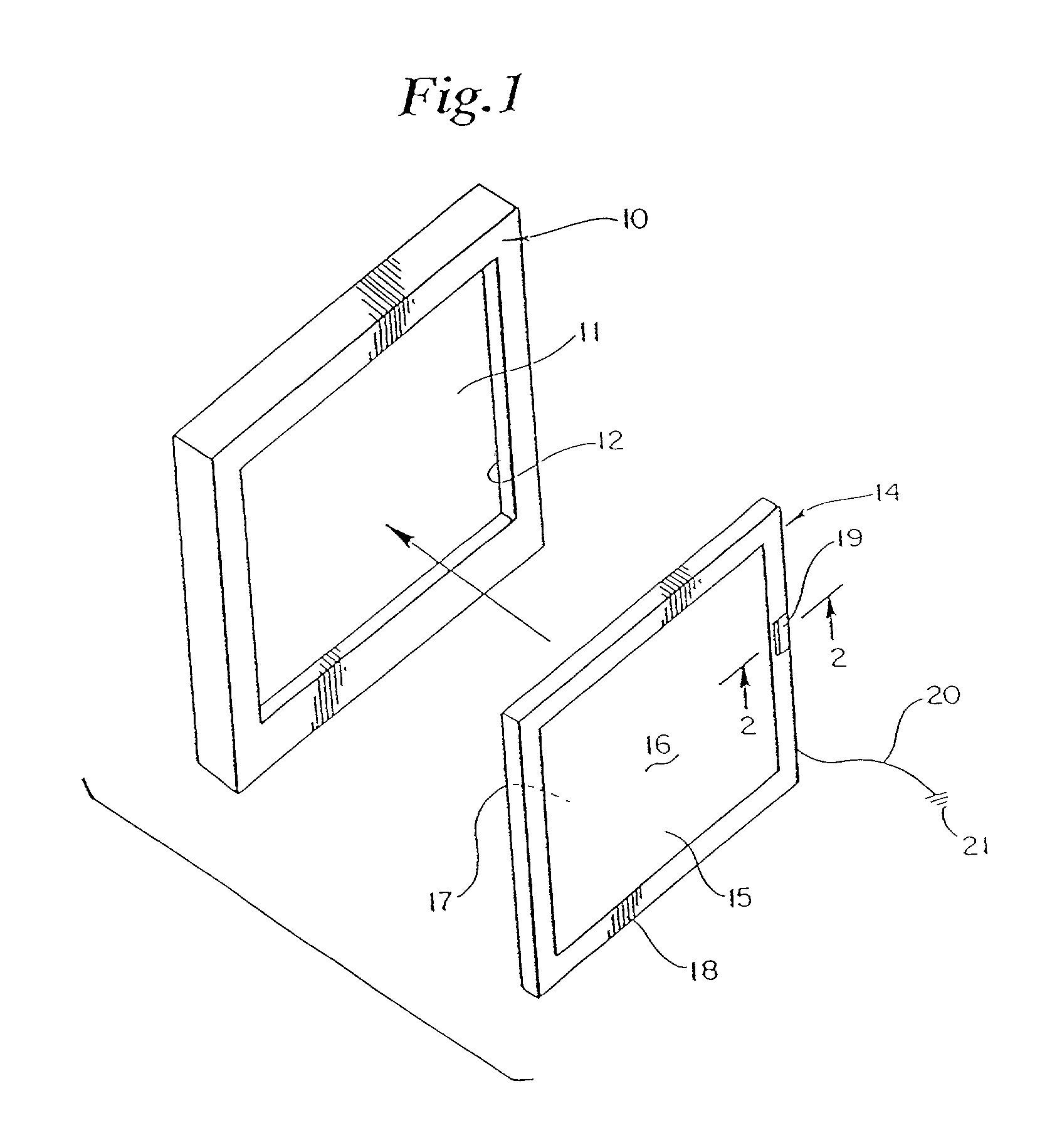
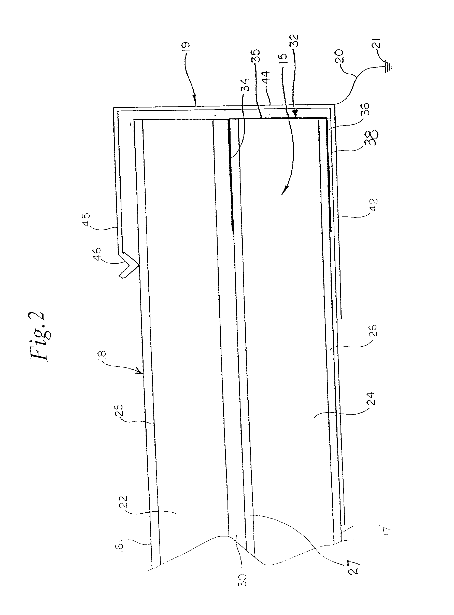
[0033] The present invention relates to a plasma display panel filter, or shielding film for use therein, which functions to provide EMI and IR shielding capabilities. Preferably the filter also provides anti-reflective (AR) capability. Various features of the present invention have possible application other than for display panel filters. However, the description of the preferred embodiment will be for use in a plasma display panel filter.

[0034] Reference is first made to FIG. 1 illustrating an exploded, isometric view of a plasma display panel 10 and associated filter 14 in accordance with the present invention. The display panel 10 as illustrated in FIG. 1 in accordance with the preferred embodiment is a generally rectangular configured device having a front viewing or display screen 11 and a recessed area 12 for receiving a display panel filter 14. It should be understood, however, that the possible relationships between a plasma display panel and a filter in accordance with th...


PUM

PropertyMeasurementUnit
thicknessaaaaaaaaaa
thicknessaaaaaaaaaa
thicknessaaaaaaaaaa

Abstract

The present invention provides a device in the form of a filter which is useable in conjunction with a plasma display panel, which is applied to the front face of a display, and which functions to reduce reflection after assembly to acceptable levels, to increase contrast enhancement ratios, to reduce EMI emissions to levels which comply with consumer safety regulations and with military and aircraft standards and to reduce infrared transmission in the 800 nm-1000 nm range to a level which does not interfere with IR remote control operation. The present invention also relates to a method of making such a plasma display panel filter and device.

Description

[0001] This application claims the benefit of Provisional Application Serial No. 60 / 116,562 filed Jan. 21, 1999.[0002] The present invention relates generally to a display panel filter, and more particularly to a filter having particular application for use with a plasma display panel or flat panel display. The present invention also relates to an IR / EMI filter film applied to a substrate for use in a display panel filter or otherwise and a method of making such a film and a display panel filter. The invention also relates to applying the display panel filter directly to a display panel and laminating the optical film between a pair of substrates in which one is a thin plastic film such as PET or other optical film.DESCRIPTION OF THE PRIOR ART[0003] Visual display panels commonly known as plasma display panels or flat panel displays have been recently introduced for the purpose of displaying visual images or information on relatively large, flat screens. Plasma display panel technol...

Claims


Application Information

Patent Timeline
Patent Type & Authority Applications(United States)
IPC IPC(8): B32B7/02G02B5/22B32B17/10C03C17/36G02B1/115G02B1/16G09F9/00H01J29/89H04N5/72
CPCB32B7/02Y10T428/24975B32B17/10174B32B17/10761B32B17/10834C03C17/36C03C17/3618C03C17/3639C03C17/3642C03C17/3644C03C17/3652C03C17/3676C03C2217/78C03C2218/365G02B1/116H01J29/896H01J2211/446B32B17/10073B32B2457/204B32B2311/08B32B2307/204B32B2307/202
Inventor WOODRUFF, DANIEL P.KOKOSCHKE, JEFFREY L.
Owner WOODRUFF DANIEL P
Why Eureka
Try Eureka