First-in first-out memory device and method of generating flag signal in the same

a memory device and flag signal technology, applied in the field of first-in-first-out memory devices and generating flag signals in, can solve the problems of long interval tempty between the generating time of a write clock signal and the generating time of a full flag signal, and is not suitable for a high-speed system

Inactive Publication Date: 2002-06-27
SAMSUNG ELECTRONICS CO LTD
View PDF0 Cites 19 Cited by
  • Summary
  • Abstract
  • Description
  • Claims
  • Application Information

AI Technical Summary

Problems solved by technology

However, since the flag generating circuit of the conventional FIFO memory device generates the full flag signal Full by comparing the current write address with the current read address, there is a problem in that an interval TFull between a write clock signal generating time and a full flag signal generating time point is long.
However, since the flag generating circuit of the conventional FIFO memory device generates the empty flag signal Empty by comparing the current write address with the current read address, there is a problem in that an interval TEmpty between a read clock signal generating time and an empty flag signal generating time point is long.
That is, the flag generating circuit of the conventional FIFO memory device generates flag signals after the current write address or the current read address is generated and thus is not suitable for a high-speed system.

Method used


Image

  • First-in first-out memory device and method of generating flag signal in the same
  • First-in first-out memory device and method of generating flag signal in the same
  • First-in first-out memory device and method of generating flag signal in the same

Examples


Embodiment Construction

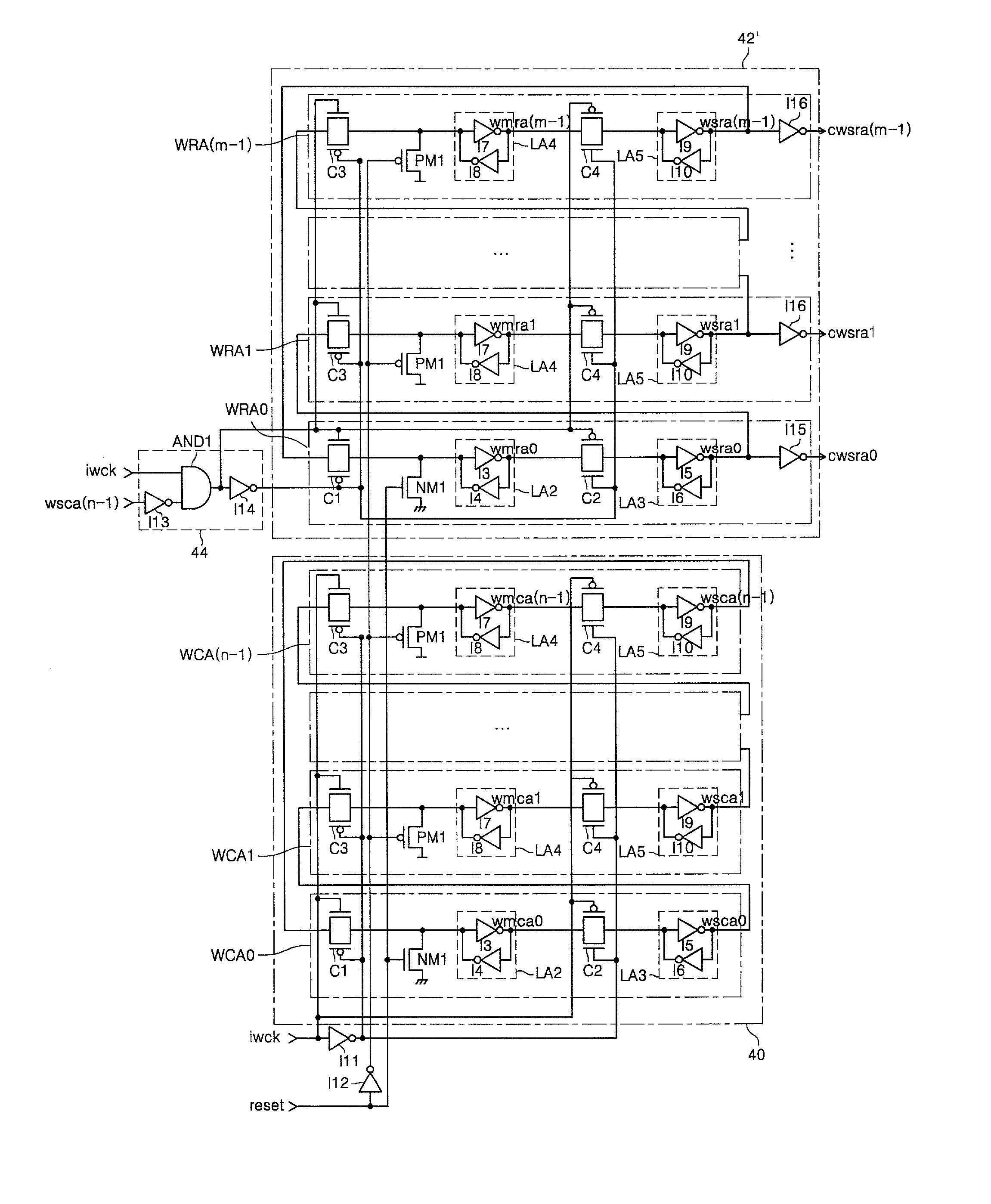
[0056] FIG. 9 is a circuit diagram illustrating a configuration of a write address generating circuit according to an embodiment of the present invention. The write address generating circuits of FIGS. 4 and 9 have analogous configurations, with the exception of the write row address generating circuit 42'. The write row address generating circuit 42' includes an inverter I15 added to the registers WRA0 and an inverter I16 added to each of the registers WRA1 to WRA(m-1) in comparison to the write row address generating circuit 42 of FIG. 4.

[0057] The inverter I15 of the register WRA0 inverts the write slave row address wsra0 to generate the address cwsra0 . Each of the inverters I16 of the register WRA1 to WRA(m-1) inverts the write slave row addresses wsra1 to wsra(m-1), respectively, to generate the addresses cwsra1 to cwsra(m-1). The inverters I15 and I16 generate, in advance, a next write master row address at a current state. That is, added inverters I15 and I16 allow the next ...


PUM


Abstract

A FIFO memory device includes a write address generating means generating a write address in response to a write clock signal and a read address generating means generating a read address in response to a read clock signal. A memory cell array includes a plurality of memory cells arranged between a plurality of write and read word lines and a plurality of write and read bit lines, the memory cell array storing write data in response to the write address and outputting read data in response to the read address. A flag signal generating means compares a next write address with a current read address to generate a full flag signal in response to the write clock signal when the next write address and the current read address are equal, and compares a current write address with a next read address to generate an empty flag signal in response to the read clock signal when the current write address and the next read address are equal.

Description

CROSS REFERENCE[0001] This application claims the benefit of Korean Patent Application No. 2000-82094, filed on Dec. 26, 2000, under 35 U.S.C. .sctn.119, the entirety of which is hereby incorporated by reference.[0002] 1. Field of the Invention[0003] The present invention relates to a first-in first-out (FIFO) memory device and a method of generating a flag signal in the same.[0004] 2. Description of Related Art[0005] In communication between different processors (or systems) having different data rates, there generally exists a difference between the speed at which one processor (or system) writes data and the speed at which the other processor (or system) reads data. The first-in first-out (FIFO) memory device is used to control data transmission between different processors having different data rate.[0006] FIG. 1 is a block diagram illustrating data transmission between processors according to conventional art. Processors 10 and 12 and a FIFO memory device 14 are shown. As shown...

Claims


Application Information

Patent Timeline
Patent Type & Authority Applications(United States)
IPC IPC(8): G06F5/14G06F12/02G11C7/10
CPCG11C7/1018G06F5/14G06F12/02
Inventor LEE, YOUNG JULIM, JEUNG JOO
Owner SAMSUNG ELECTRONICS CO LTD
Why Eureka
Try Eureka