Methods and apparatus for processing the surface of a microelectronic workpiece

a microelectronic workpiece and surface technology, applied in the direction of electrolysis components, manufacturing tools, coatings, etc., can solve the problems of increasing maintenance requirements, non-uniform deposition of plated metallic materials, and increasing the complexity of electroplating equipment, so as to reduce the risk of contamination

Inactive Publication Date: 2002-08-15
SEMITOOL INC
View PDF0 Cites 35 Cited by
  • Summary
  • Abstract
  • Description
  • Claims
  • Application Information

AI Technical Summary

Benefits of technology

[0023] In accordance with a further aspect of the present invention, the contact assembly is connected within the reactor assembly by one rmore latching mechanisms. The latching mechanisms allow easy replacement of the contact assembly with another contact assembly of the same or of a different type. Given the construction of the disclosed contact assemblies, replacement with the same type of contact assembly reduces or otherwise eliminates the need for recalibration of the plating system thereby reducing down time of the reactor.
[0025] The reactor as may also include a backing member and a drive mechanism in an assembly in which the backing member and contact assembly are moved relative to one another by the drive mechanism between a workpiece loading state and a workpiece processing state. In the workpiece processing state, the workpiece is urged against the plurality of contacts of the contact assembly by the backing member. To reduce the risk of contamination from particles released by the drive mechanism, the drive mechanism may be substantially surrounded by a bellows member.

Problems solved by technology

This non-uniform distribution of current across the wafer, in turn, causes non-uniform deposition of the plated metallic material.
But such thieving techniques add to the complexity of electroplating equipment, and increase maintenance requirements.
Another problem with electroplating of wafers concerns efforts to prevent the electric contacts themselves from being plated during the electroplating process.
While it is possible to provide sealing mechanisms for discrete electrical contacts, such arrangements typically cover a significant area of the wafer surface, and can add complexity to the electrical contact design.
Electroplated material may not adhere well to the exposed barrier layer material, and is therefore prone to peeling off in subsequent wafer processing steps.
Further, metal that is electroplated onto the barrier layer within the reactor may flake off during the electroplating process thereby adding particulate contaminants to the electroplating bath.
Such contaminants can adversely affect the overall electroplating process.
The specific metal to be electroplated can also complicate the electroplating process.
As a consequence, use of the typical plurality of electrical wafer contacts (for example, six (6) discrete contacts) may not provide adequate uniformity of the plated metal layer on the wafer.
Beyond the contact related problems discussed above, there are also other problems associated with electroplating reactors.
Still further, existing electroplating reactors are often difficult to maintain and / or reconfigure for different electroplating processes.
One drawback associated with copper deposition by electroplating is the fact that for very small features on microelectronic workpieces (sub 0.1 micron features), copper deposition by electroplating can lack conformality with the side walls of high aspect ratio vias and trenches, and can produce voids in the formed interconnects and plugs (vias).
This is often due to the non-conformality of the copper seed layer deposited by PVD or CVD as a result, the seed layer may not be thick enough to carry the current to the bottom of high aspect ratio features.

Method used


Image

  • Methods and apparatus for processing the surface of a microelectronic workpiece
  • Methods and apparatus for processing the surface of a microelectronic workpiece
  • Methods and apparatus for processing the surface of a microelectronic workpiece

Examples


Embodiment Construction

[0047] Basic Reactor Components

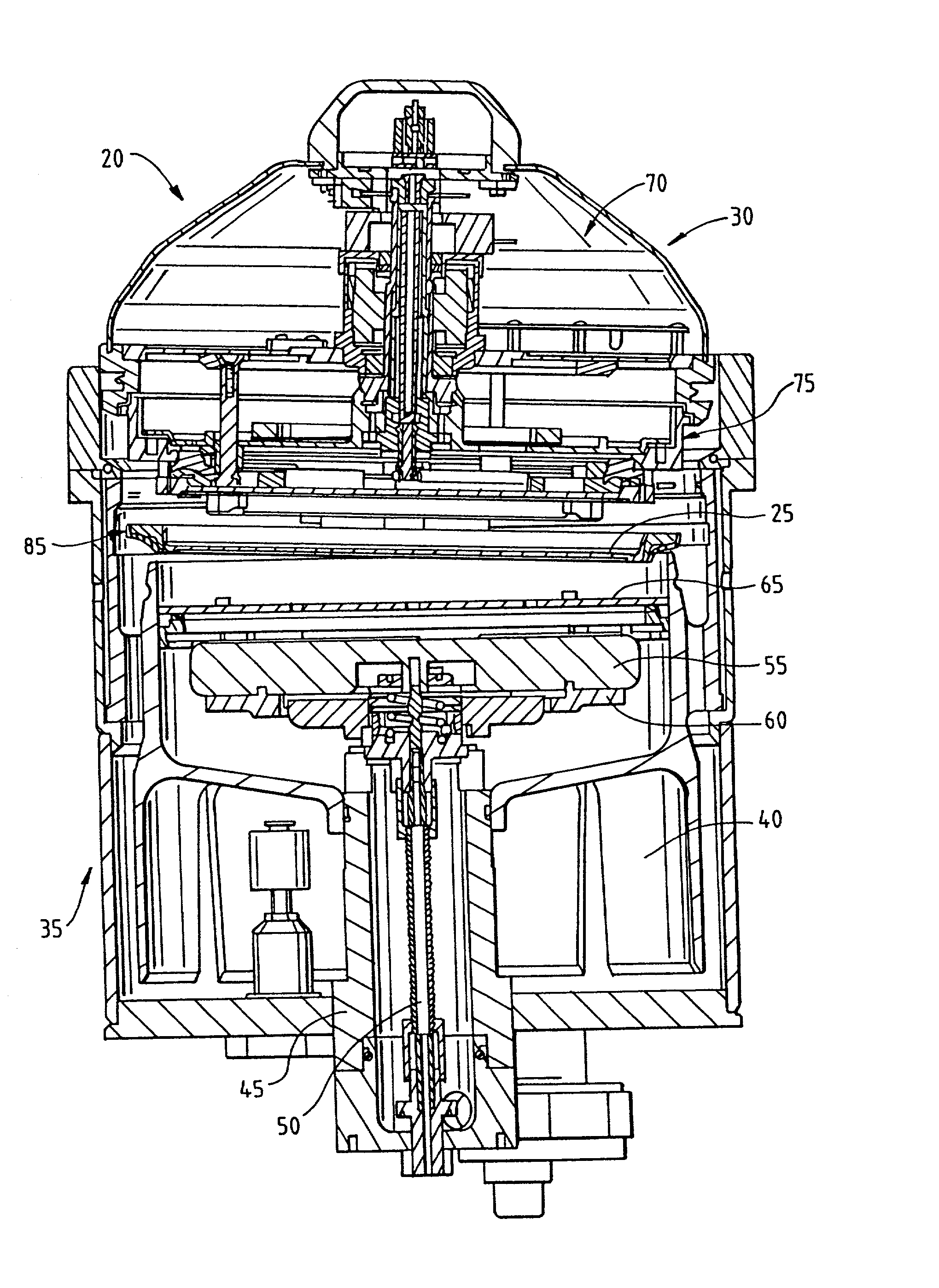
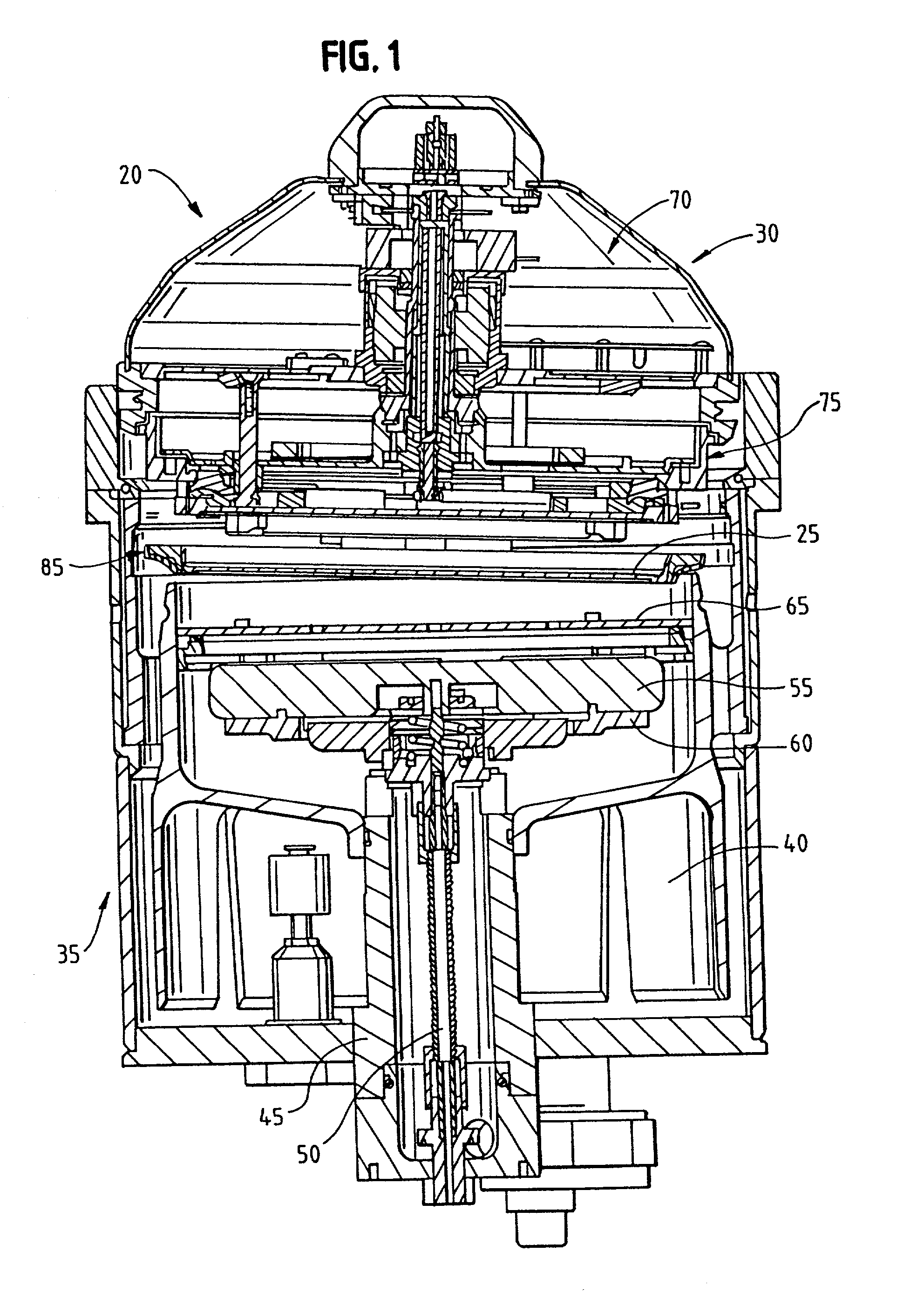
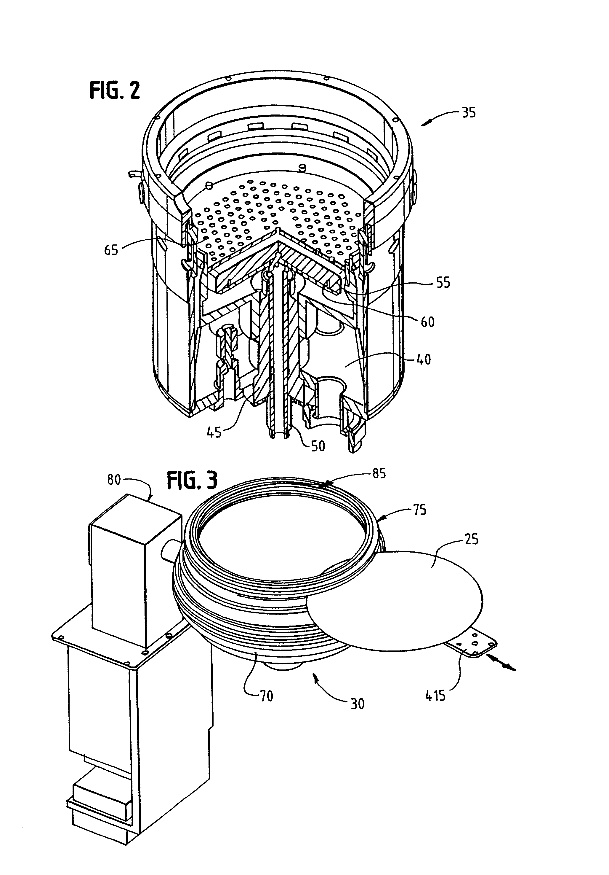
[0048] With reference to FIGS. 1-3, there is shown a reactor assembly 20 for electroplating a microelectronic workpiece, such as a semiconductor wafer 25. Generally stated, the reactor assembly 20 is comprised of a reactor head 30 and a corresponding reactor bowl 35. This type of reactor assembly is particularly suited for effecting electroplating of semiconductor wafers or like workpieces, in which an electrically conductive, thin-film layer of the wafer is electroplated with a blanket or patterned metallic layer.

[0049] The specific construction of one embodiment of a reactor bowl 35 suitable for use in the reactor assembly 20 is illustrated in FIG. 2. The electroplating reactor bowl 35 is that portion of the reactor assembly 20 that contains electroplating solution, and that directs the solution against a generally downwardly facing surface of an associated workpiece 25 to be plated. To this end, electroplating solution is circulated through the reac...


PUM

PropertyMeasurementUnit
thickaaaaaaaaaa
thicknessaaaaaaaaaa
angleaaaaaaaaaa

Abstract

A reactor for plating a metal onto a surface of a workpiece is set forth. The reactor comprises a reactor bowl including an electroplating solution disposed therein and an anode disposed in the reactor bowl in contact with the electroplating solution. A contact assembly is spaced from the anode within the reactor bowl. The contact assembly includes a plurality of contacts disposed to contact a peripheral edge of the surface of the workpiece to provide electroplating power to the surface of the workpiece. The contacts execute a wiping action against the surface of the workpiece as the workpiece is brought into engagement therewith The contact assembly also including a barrier disposed interior of the plurality of contacts. The barrier includes a member disposed to engage the surface of the workpiece to assist in isolating the plurality of contacts from the electroplating solution. In one embodiment, the plurality of contacts are in the form of discrete flexures while in another embodiment the plurality of contacts are in the form of a Belleville ring contact. A flow path may be provided in the contact assembly for providing a purging gas to the plurality of contacts and the peripheral edge of the workpiece. The purging gas may be used to assist in the formation of the barrier of the contact assembly. A combined electroplating / electroless plating tool and method are also set forth.

Description

[0001] Production of semiconductor integrated circuits and other microelectronic devices from workpieces such as semiconductor wafers typically requires formation of one or more metal layers on the wafer. These metal layers are used, for example, to electrically interconnect the various devices of the integrated circuit. Further, the structures formed from the metal layers may constitute microelectronic devices such as read / write heads, etc.[0002] The microelectronic manufacturing industry has applied a wide range of metals to form such structures. These metals include, for example, nickel, tungsten, solder, platinum, and copper. Further, a wide range of processing techniques have been used to deposit such metals. These techniques include, for example, chemical vapor deposition (CVD), physical vapor deposition (PVD), electroplating, and electroless plating. Of these techniques, electroplating and electroless plating tend to be the most economical and, as such, the most desirable. El...

Claims


Application Information

Patent Timeline
Patent Type & Authority Applications(United States)
IPC IPC(8): C25D5/08C25D7/12C25D17/06H01L21/288H01L21/687
CPCC25D5/08C25D17/06H01L21/288H01L21/2885H01L21/687H01L21/68721H01L21/68728H01L21/68735H01L21/68785C25D7/123C25D17/001
Inventor WOODRUFF, DANIEL J.HANSON, KYLE M.OBERLITNER, THOMAS H.CHEN, LINLINPEDERSEN, JOHN M.ZILA, VLADIMIR
Owner SEMITOOL INC
Why Eureka
Try Eureka