Planarization of substrates using electrochemical mechanical polishing

a technology of electrochemical mechanical polishing and substrate, applied in the direction of electrolysis components, manufacturing tools, lapping machines, etc., can solve the problems of difficult to pattern and etch copper, and difficult to achieve effective conformal removal of copper material from the substrate surfa

Inactive Publication Date: 2002-09-19
APPLIED MATERIALS INC
View PDF19 Cites 132 Cited by
  • Summary
  • Abstract
  • Description
  • Claims
  • Application Information

AI Technical Summary

Benefits of technology

0018] In another aspect, an electrochemical deposition system is provided that includes a mainframe having a mainframe wafer transfer robot, a loading station disposed in connection with the mainframe, one or more electrochemical processing cells disposed in conn

Problems solved by technology

However, copper is difficult to pattern and etch.
Additionally, substrate surfaces may have different surface topography, depending on the density or size of features formed therein, which makes effective conformal removal of copper material from the substrate surface difficult to achieve.
Additionally, the relatively uneven removal rates can result in underpolishing of areas of the substrate with residual copper material remaining after the polishing process.
However, overpolishing of some materials can result in the formation of topographical defects, such as concavities or depressions in features, referred to as dishing, or excessive removal of dielectric material, referred to as erosion.
The topographical defects from dishing and erosion can further lead to non-uniform removal of additional materials, such as barrier

Method used


Image

  • Planarization of substrates using electrochemical mechanical polishing
  • Planarization of substrates using electrochemical mechanical polishing
  • Planarization of substrates using electrochemical mechanical polishing

Examples


Embodiment Construction

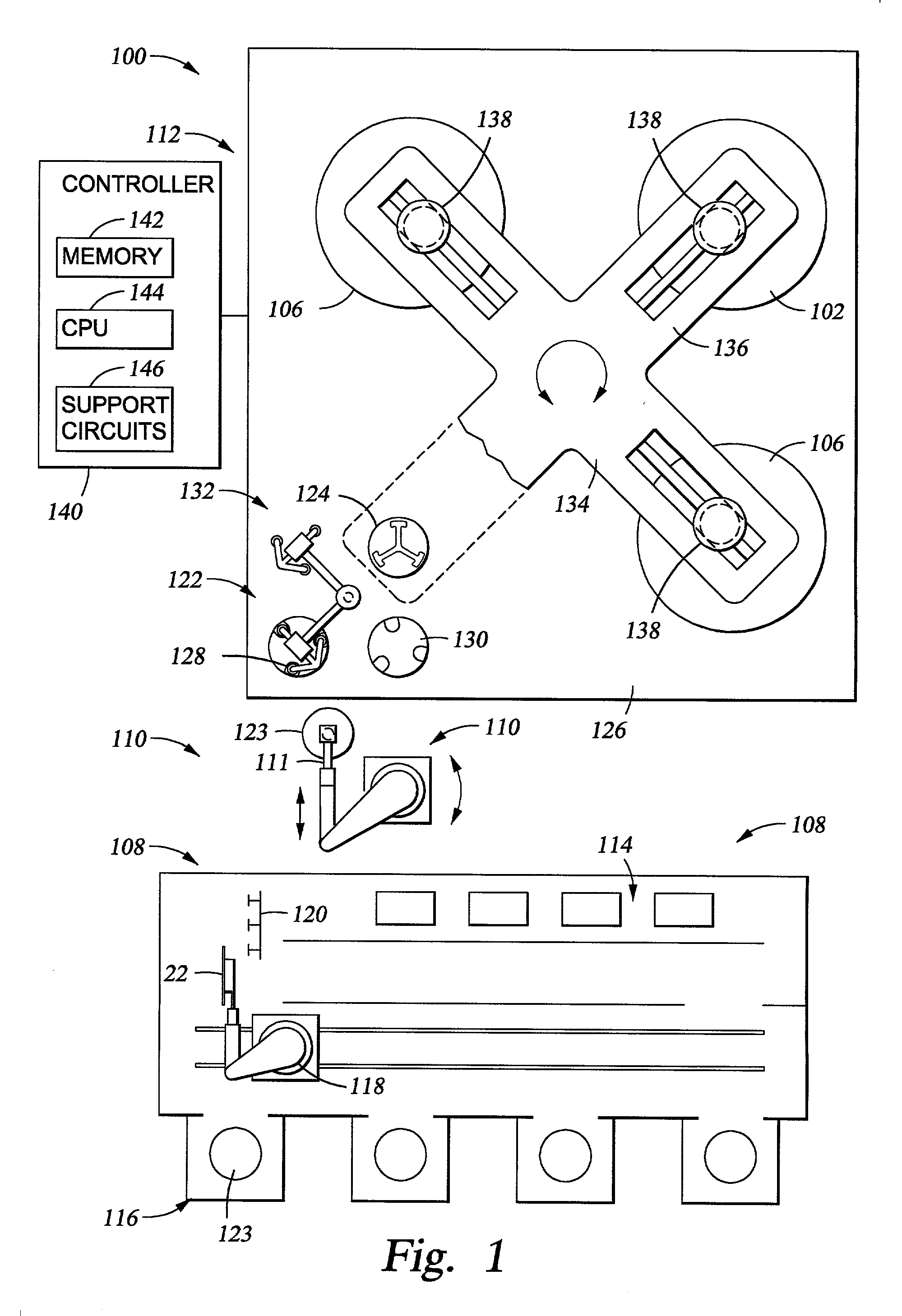
[0035] In general, aspects of the invention provide apparatus and methods for planarizing a substrate surface with reduced contact pressure between a substrate and a polishing apparatus. The invention will be described below in reference to a planarizing process for the removal of conductive materials, such as copper and other copper containing materials from a substrate surface by electrochemical mechanical polishing (ECMP) techniques.

[0036] The words and phrases used herein should be given their ordinary and customary meaning in the art by one skilled in the art unless otherwise further defined. Chemical-mechanical polishing should be broadly construed and includes, but is not limited to, abrading a substrate surface by chemical activity, mechanical activity, or a combination of both chemical and mechanical activity. Electropolishing should be broadly construed and includes, but is not limited to, removing material from a substrate by the application of electrochemical activity, s...


PUM

PropertyMeasurementUnit
Pressureaaaaaaaaaa
Electric potential / voltageaaaaaaaaaa

Abstract

A method and apparatus are provided for planarizing a material layer on a substrate. In one aspect, a method is provided for processing a substrate including forming a passivation layer on a substrate surface, polishing the substrate in an electrolyte solution, applying an anodic bias to the substrate surface, and removing material from at least a portion of the substrate surface. In another aspect, an apparatus is provided which includes a partial enclosure, polishing article, a cathode, a power source, a substrate carrier movably disposed above the polishing article, and a computer based controller to position a substrate in an electrolyte solution to form a passivation layer on a substrate surface, to polish the substrate in the electrolyte solution with the polishing article, and to apply an anodic bias to the substrate surface or polishing article to remove material from at least a portion of the substrate surface.

Description

CROSS-REFERENCE TO RELATED APPLICATIONS[0001] This application claims benefit of U.S. Provisional Patent Application Serial No. 60 / 275,874, filed on Mar. 14, 2001, U.S. Provisional Patent Application Serial No. 60 / 286,107, filed on Apr. 24, 2001, and U.S. Provisional Patent Application Serial No. 60 / 326,263, filed Oct. 1, 2001, each of which are incorporated herein by reference.BACKGROUND OF THE INVENTION[0002] 1. Field of the Invention[0003] The present invention relates to an apparatus and method for planarization of a material, such as a metal, on a substrate.[0004] 2. Background of the Related Art[0005] Sub-quarter micron multi-level metallization is one of the key technologies for the next generation of ultra large-scale integration (ULSI). The multilevel interconnects that lie at the heart of this technology require planarization of interconnect features formed in high aspect ratio apertures, including contacts, vias, lines and other features. Reliable formation of these inter...

Claims


Application Information

Patent Timeline
IPC IPC(8): B23H5/08B24B37/04B24B37/00H01L21/304H01L21/316
CPCB23H5/08H01L21/304
Inventor CHEN, LIANG-YUHHSU, WEI-YUNGDUBOUST, ALAINMORAD, RATSONCARL, DANIEL A.
Owner APPLIED MATERIALS INC
Why Eureka
Try Eureka