Transistor

a transistor and transistor technology, applied in the field of transistors, can solve the problems of limiting the degree of integration of silicon devices, unstable operation of transistors, and extremely difficult industrial use of transistors, and achieve the effect of reducing the size of electronic circuits

Inactive Publication Date: 2002-09-19
FUJIFILM BUSINESS INNOVATION CORP
View PDF0 Cites 43 Cited by
  • Summary
  • Abstract
  • Description
  • Claims
  • Application Information

AI Technical Summary

Benefits of technology

0008] An object of the present invention is to provide extremely small transistor which can correspond to significant reduction in the size of an electronic circuit by using DNA as structural materials. The present invention discloses a transistor comprising a source electrode member; a drain electrode member; a

Problems solved by technology

There is a limit to the degree of integration of a silicon device which is now widely used in view of its working.
If a gate width of a silicon field effect transistor is 100 nm or less, the transistor is considered to be extremely difficult to use industrially.
A

Method used


Image

  • Transistor
  • Transistor
  • Transistor

Examples


embodiment (

[0069] Embodiment (2)

[0070] In Embodiment (2), deoxyribonucleic acid molecule or deoxyribonucleic acid molecule aggregate in a form of mass to connect to gate electrode member, and acts as an insulating material.

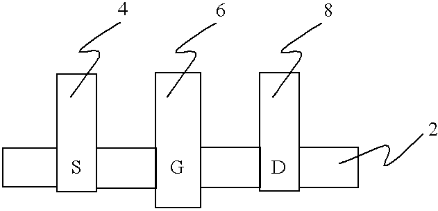
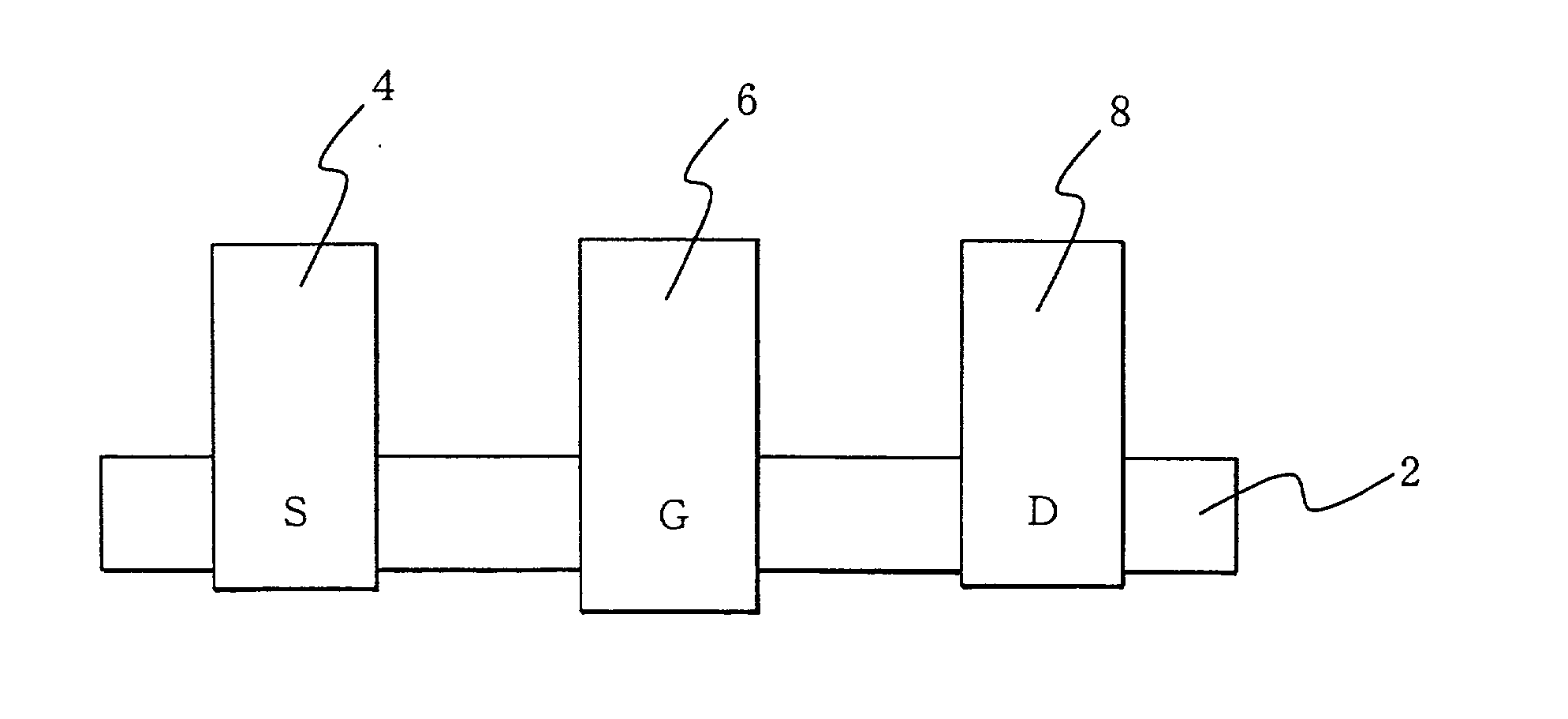
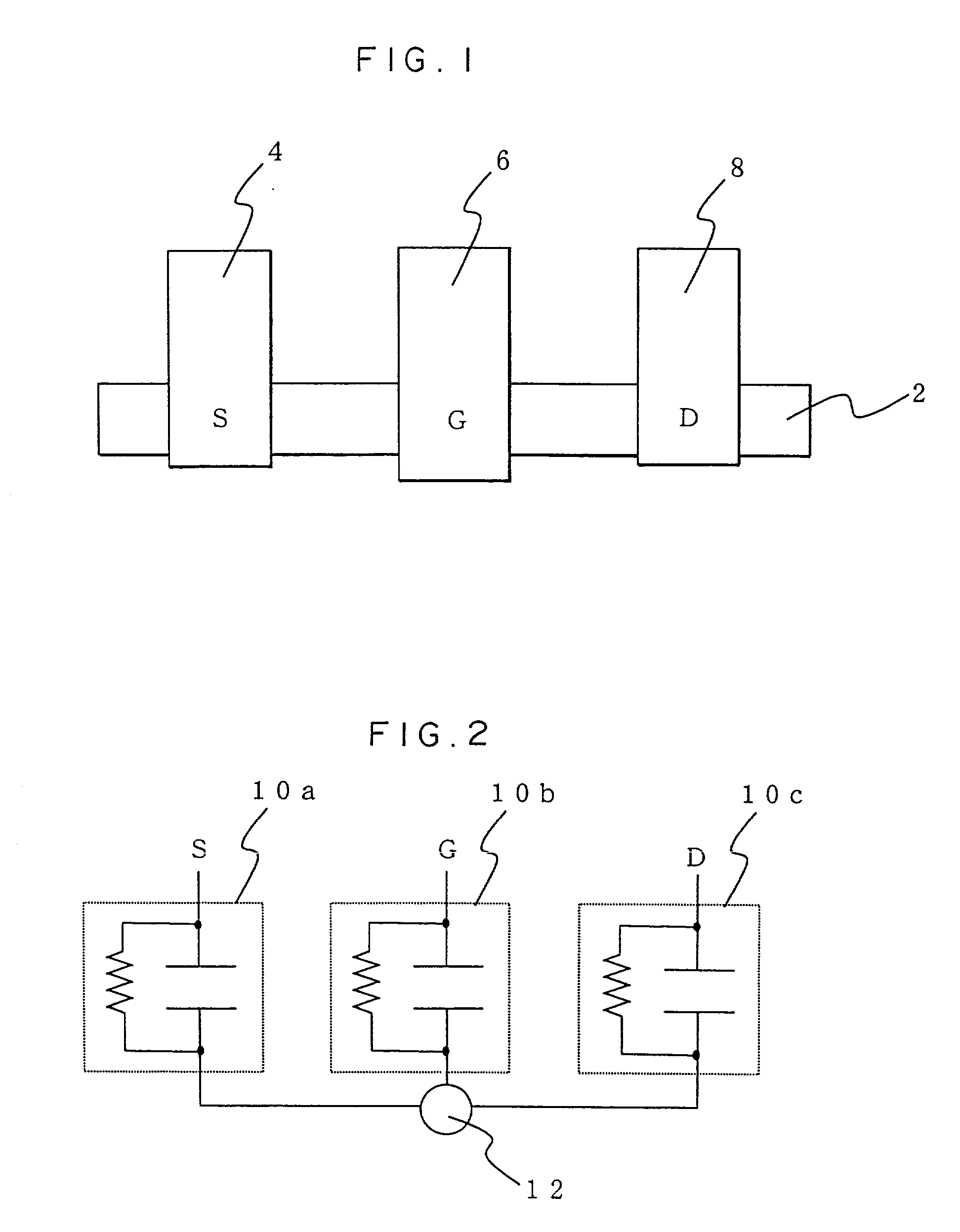
[0071] FIG. 3 shows a typical structural view of Embodiment (2) of the present invention. In FIG. 3, reference numeral 20 designates a carrier transporting material. A block of deoxyribonucleic acid molecule (DNA) 22 is disposed on the carrier transporting material 20 and contacts it. A gate electrode member 26 connects to the DNA 22 not so as to contact the carrier transporting member 20.A source electrode member 24 and a drain electrode member 28 are disposed at both sides of the DNA 22 with the gate electrode member 26 being disposed therebetween. In this way, a transistor is formed. A strong depletion layer is formed in the carrier transporting material 20 because of the existence of the DNA 22 such that the transistor acts as a field effect transistor.

[0072] The same DN...

example 1

[0080] In Example 1, DNA that was taken from sperm of a natural salmon was used. In order to remove impurities such as protein and the like from the DNA, 10 mg of crude-extracted DNA was dispersed in 10 ml of ethanol (99.9% by weight). The resultant mixture was stirred at room temperature for 30 minutes and filtered by a PTFE filter with pores having a diameter of 1 .mu.m. This operation was repeated three times. Then, the resultant DNA from which protein had been removed was dispersed in 100 ml of a buffer solution (sodium chloride: 300 mmol / L, sodium carbonate: 10 mmol / L, EDTA: 5 mmol / L). Ultrapure water (resistance value: 1.83 M.OMEGA.) was used for preparing the buffer solution. The resultant mixture was stirred at room temperature for 30 minutes and filtered by a polytetrafluoroethylene (PTFE) filter with pores having a diameter of 1 .mu.m. Thus, impurities were removed from the DNA.

[0081] Next, in order to remove salts from the DNA, the DNA was dispersed in a mixed solution of...


PUM


Abstract

There is provided a transistor, which includes a deoxyribonucleic acid molecule or a deoxyribonucleic acid molecule aggregate as a part of structural materials, has a source electrode member, a drain electrode member and a gate electrode member, in which at least one of three electrode members connects to the deoxyribonucleic acid molecule or deoxyribonucleic acid molecule aggregate 1

Description

BACKGROUND OF THE INVENTION[0001] 1. Field of the Invention[0002] The present invention relates to a transistor, and in particular, to an extremely small transistor which can correspond to significant reduction in the size of an electronic circuit.[0003] 2. Description of the Related Art[0004] There is a limit to the degree of integration of a silicon device which is now widely used in view of its working. If a gate width of a silicon field effect transistor is 100 nm or less, the transistor is considered to be extremely difficult to use industrially. Also, if it is thought that, as a principle, if the gate width of a transistor is 20 nm or less, an operation of the transistor becomes unstable because of a tunnel effect or the like. Accordingly, a molecular device which uses a functional molecule itself such as carbon nanotube, Fullerene or the like is being developed as an electronic device material for replacing silicon.[0005] Meanwhile, a function of deoxyribonucleic acid (which ...

Claims


Application Information

Patent Timeline
IPC IPC(8): H01L21/336H01L21/28H01L29/06H01L29/43H01L29/66H01L29/78H01L29/786H01L51/05H01L51/30
CPCB82Y10/00G11C13/0014G11C13/0019G11C2213/17H01L51/0093H01L51/0508Y10S977/936H10K85/761H10K10/46
Inventor WATANABE, HIROYUKIMANABE, CHIKARASHIGEMATSU, TAISHISHIMOTANI, KEISHIMIZU, MASAAKI
Owner FUJIFILM BUSINESS INNOVATION CORP
Why Eureka
Try Eureka