Optical integrated circuit and method for manufacturing optical integrated circuit

a technology of optical integrated circuits and integrated circuits, applied in the direction of optical waveguide light guides, optical elements, instruments, etc., can solve the problems of large radiation loss of light propagating an optical waveguide layer, clad layer is liable to be cracked at its step portion, and increased cos

Inactive Publication Date: 2002-09-19
PIONEER CORP
View PDF3 Cites 20 Cited by
  • Summary
  • Abstract
  • Description
  • Claims
  • Application Information

AI Technical Summary

Problems solved by technology

A wave-guide path type photo-detector construction by use of an optical IC substrate having such a configuration, however, has suffered from a problem that, as shown in FIG. 7, an insulator film layer and a light-blocking film layer are formed as stacked on the substrate to thereby form a steep step with a value on the micrometer order at a boundary between a photo-detecting portion and such a portion of the light-blocking film layer that surrounds the photo-detecting portion, so that the resultant bent portion has a large radiation loss of the light propagating an optical wave-guide layer.
Furthermore, since this step is step, a clad layer is liable to be cracked at its step portion, which constitutes another problem.
Further, to polish such a steep step at the boundary of the light-blocking film layer for improvement of the performance, the costs are increased, which constitutes a further problem.
Those problems become more remarkable as the numbers of the insulator film layers and the light-blocking film layers increase when the optical IC employs a multi-layer wiring configuration.

Method used


Image

  • Optical integrated circuit and method for manufacturing optical integrated circuit
  • Optical integrated circuit and method for manufacturing optical integrated circuit
  • Optical integrated circuit and method for manufacturing optical integrated circuit

Examples


Embodiment Construction

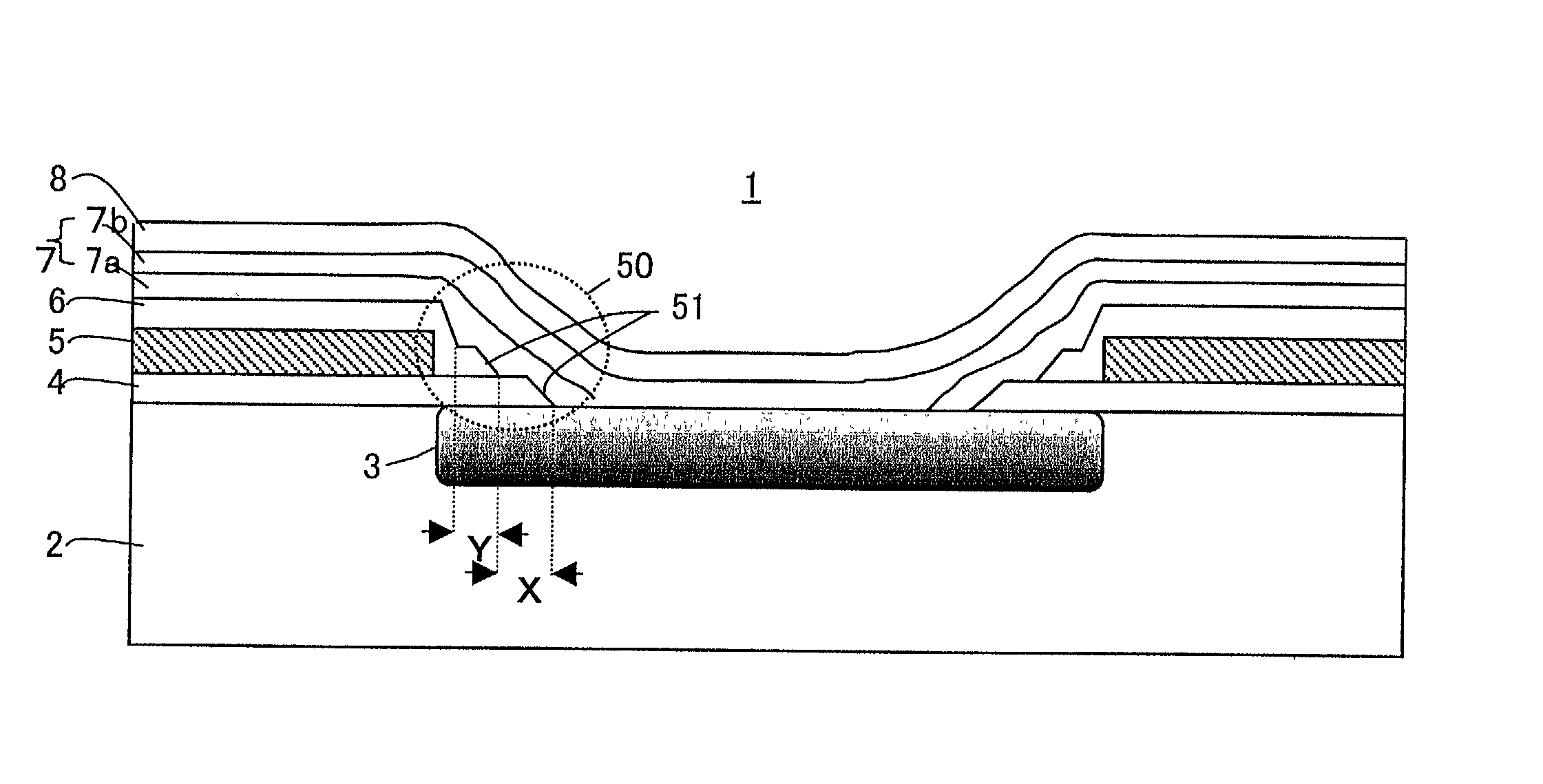
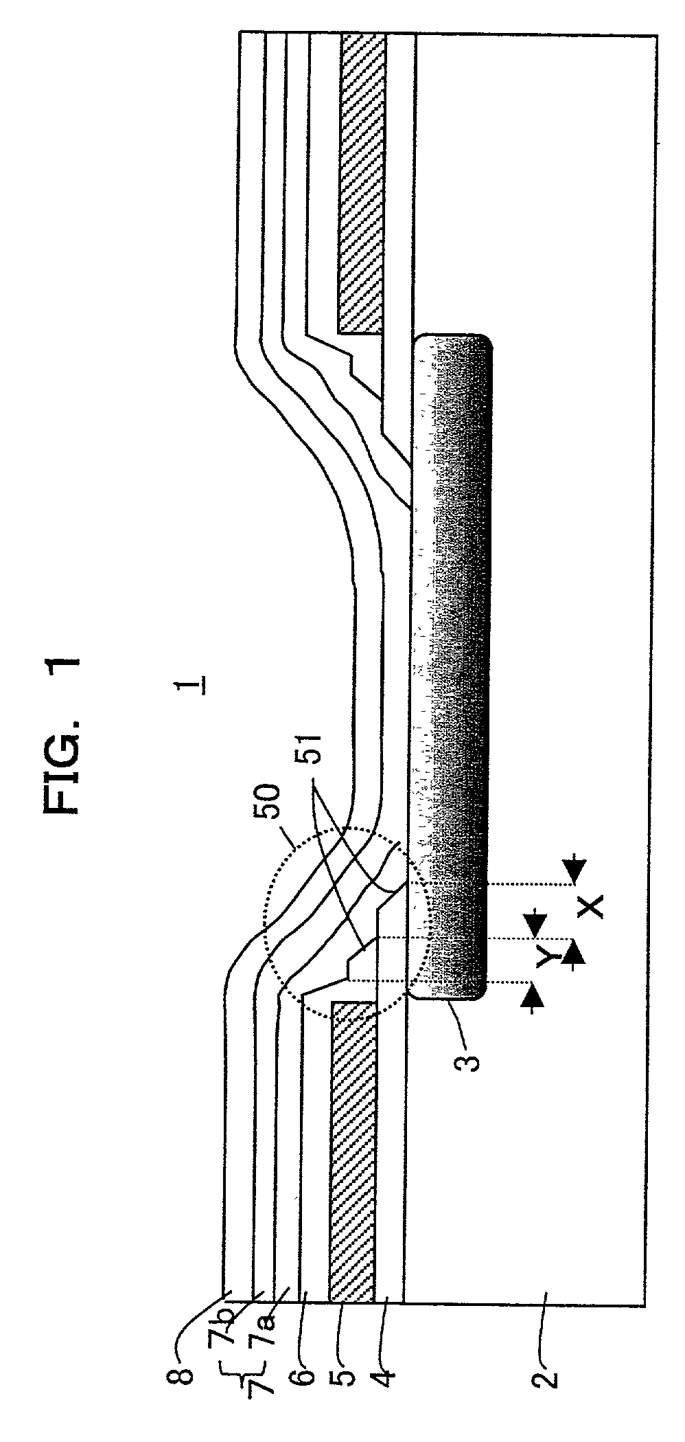
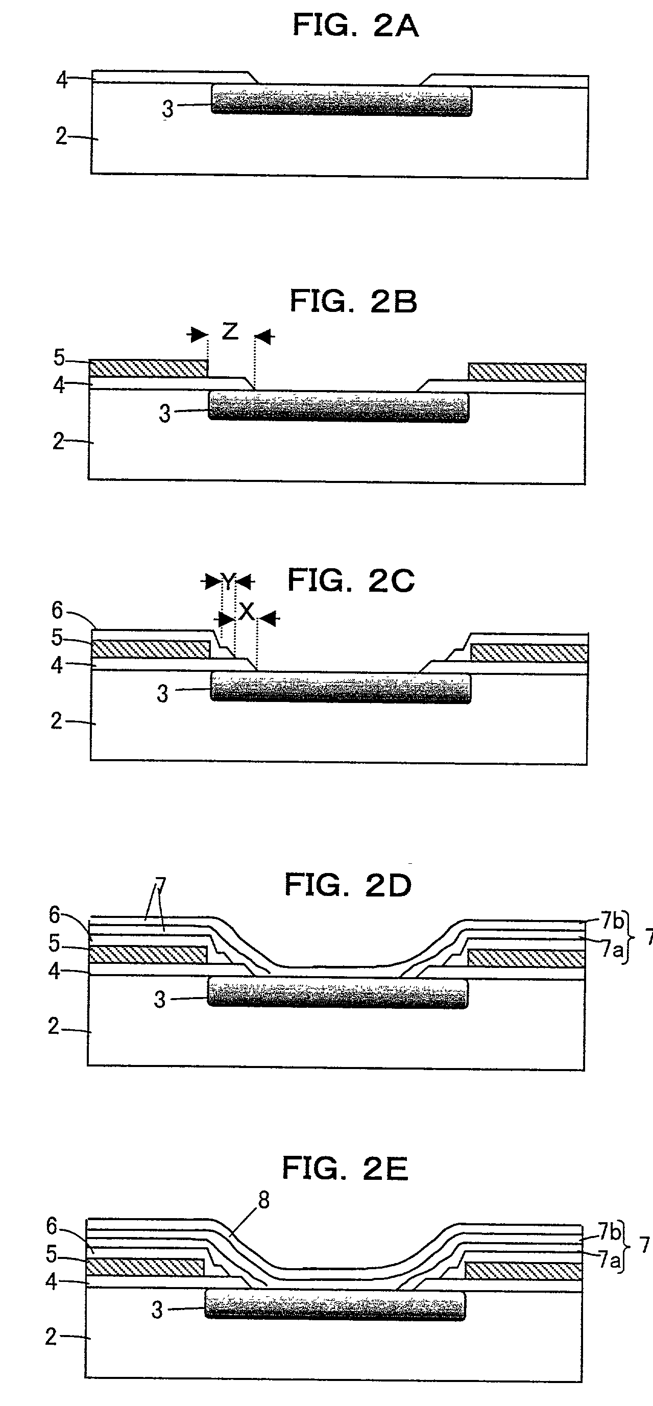
[0039] The following will describe preferred embodiments of the present invention with reference to the drawings. First, a configuration etc. of an optical IC according to an embodiment of the present invention with reference to FIG. 1.

[0040] FIG. 1 shows an example of a cross-sectional construction of an optical IC according to the embodiment of the present invention. An optical IC 1 comprises a photo-detector 3 formed on part of the main surface of a silicon (Si) substrate 2, a light-blocking film layer 5 formed on the portions other than that where the photo-detector 3 is formed, a first insulator film layer 4 and a second insulator film layer 6 formed so as to sandwich the light-blocking film layer 5 therebetween, a clad layer 7 formed on the photo-detector 3 and the insulator film layers 4 and 6, and an optical wave-guide path layer 8 formed on the clad layer 7.

[0041] In the example of FIG. 1, the first insulator film layer 4 pushes out over the photo-detector 3, the end face o...


PUM


Abstract

The present invention discloses an optical IC including a photo-detector formed on a substrate, at least one light-blocking film layer formed in a portion of the main surface of the substrate other than the portion where the light-detector is formed, at least two insulator film layers formed so as to cover the light-blocking film layer, a clad layer formed consecutively over the photo-detector and the insulator film layers, and an optical wave-guide path layer formed on the clad layers, in which the insulator film layers are formed so as to form a plurality of staircase-like steps toward the photo-detector.

Description

[0001] 1. Field of the Invention[0002] The present invention relates to an optical integrated circuit (IC) and method for manufacturing the same and, more particularly to, such an optical IC and method for manufacturing the same that can reduce a scatter loss of an optical signal.[0003] 2. Description of the Related Art[0004] In a conventional optical IC practically used in optical pick-up or optical-fiber communication, typically an optical element such as a lens is used to guide a light which has propagated a space, to then detect it by a photo-detector.[0005] Such a optical IC, however, is expected to be of a wave-guide path type so as to reduce the number of the optical elements used therein and hence the costs thereof as well as to have more functions by use of, for example, an electro-optic effect. FIG. 7 is a cross-sectional view for showing one example of a configuration of a wave-guide path type photo-detector which is manufactured on the optical IC substrate. As shown in F...

Claims


Application Information

Patent Timeline
Patent Type & Authority Applications(United States)
IPC IPC(8): G02B6/122G02B6/132G02B6/42H01L31/0232
CPCG02B6/132G02B6/4203
Inventor ONOE, ATSUSHI
Owner PIONEER CORP
Why Eureka
Try Eureka