Fabrication of molecular electronic circuit by imprinting
What is AI technical title?
AI technical title is built by Patsnap AI team. It summarizes the technical point description of the patent document.
a technology of electronic circuits and imprints, which is applied in the manufacture of semiconductor devices, electrical devices, nanostructures, etc., can solve the problems of increasing manufacturing difficulty, increasing design difficulty, and increasing cost, and achieve the effect of avoiding damage to the devi
Inactive Publication Date: 2003-01-02
HEWLETT PACKARD DEV CO LP
View PDF0 Cites 28 Cited by
Summary
Abstract
Description
Claims
Application Information
AI Technical Summary
This helps you quickly interpret patents by identifying the three key elements:
Problems solved by technology
Method used
Benefits of technology
Benefits of technology
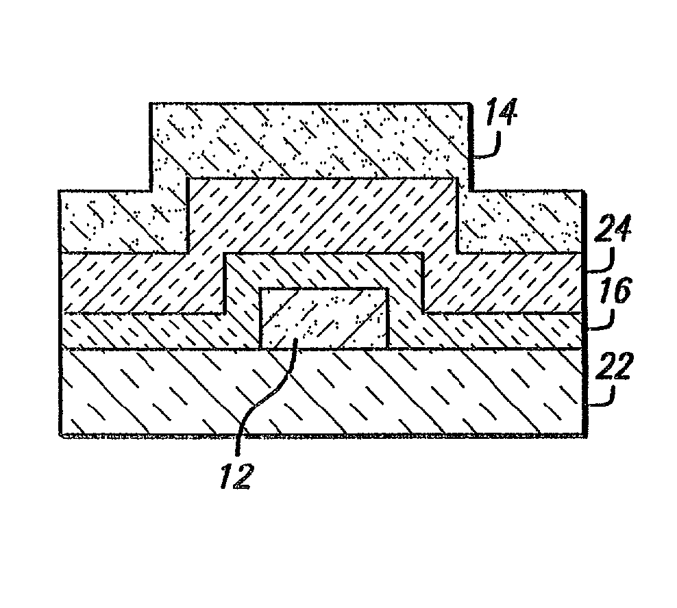
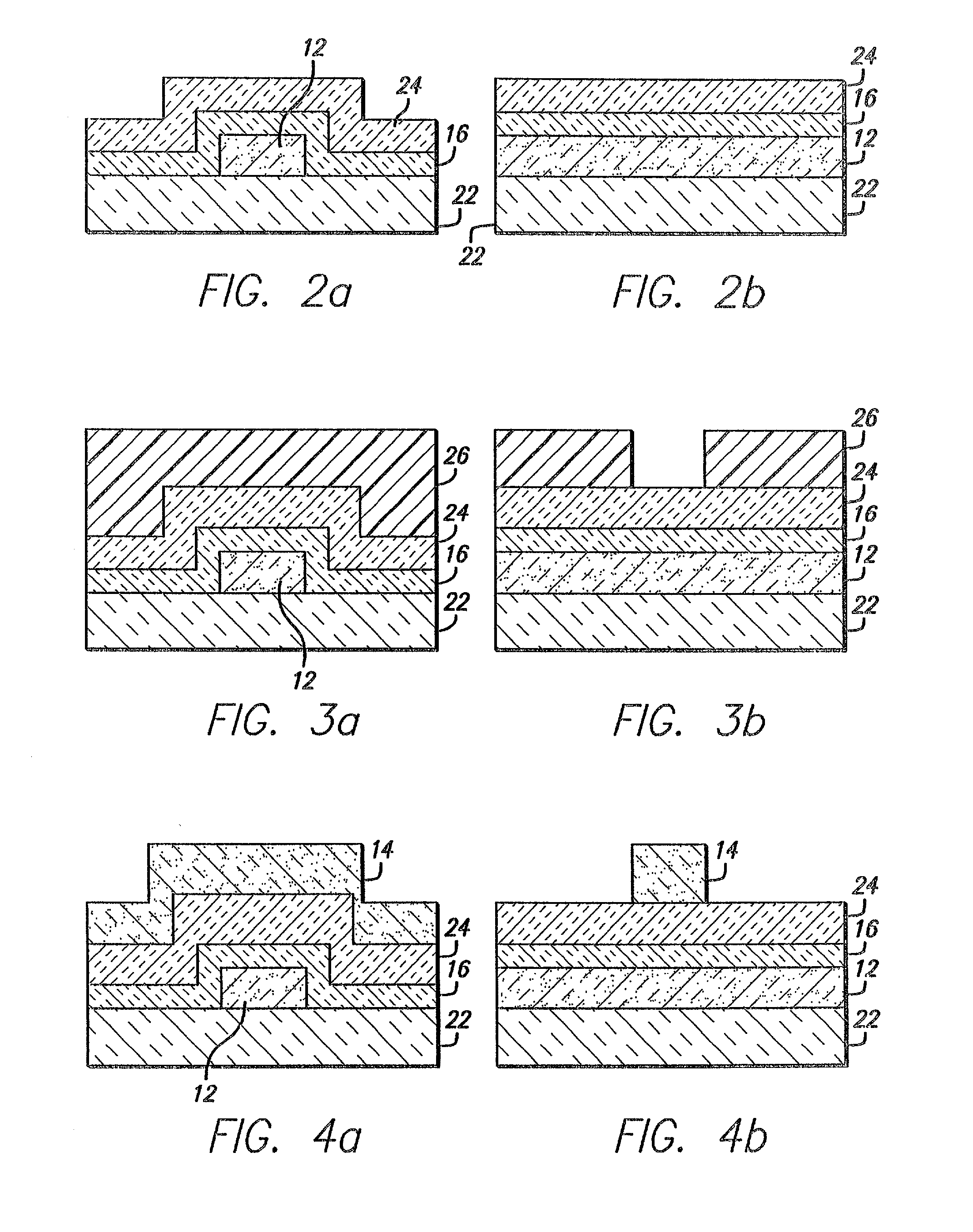
[0013] (c) forming a protective layer on top of the molecular switch film to avoid damage thereto during further processing;
Problems solved by technology
With the constantly decreasing feature sizes of integrated-circuit devices, well-behaved devices are becoming increasingly difficult to design.
The fabrication is also becoming increasingly difficult and expensive.
Method used
Image
Click on the blue label to locate the original text in one second.
Reading with bidirectional positioning of images and text.
Examples
Embodiment Construction
[0022] Definitions
[0023] As used herein, the term "self-aligned" as applied to "junction" means that the junction that forms the switch and / or other electrical connection between two wires is created wherever two wires, either of which may be coated or functionalized, cross each other, because it is the act of crossing that creates the junction.
[0024] The term "self-assembled" as used herein refers to a system that naturally adopts some regular pattern because of the identity of the components of the system; the system achieves at least a local minimum in its energy by adopting this configuration.
[0025] The term "singly configurable" means that a switch can change its state only once via an irreversible process such as an oxidation or reduction reaction; such a switch can be the basis of a programmable read-only memory (PROM), for example.
[0026] The term "reconfigurable" means that a switch can change its state multiple times via a reversible process such as an oxidation or reductio...
PUM
Abstract
A method of fabricating a molecular electronic device or crossbar memory device is provided. The device comprises at least one pair of crossed wires and a molecular switch film therebetween. The method comprises: (a) forming at least one bottom electrode on a substrate by first forming a first layer on the substrate and patterning the first layer to form the bottom electrode by an imprinting technique; (b) forming the molecular switch film on top of the bottom electrode; (c) optionally forming a protective layer on top of the molecular switch film to avoid damage thereto during further processing; (d) coating a polymer layer on top of the protective layer and patterned the polymer layer by the imprinting method to form openings that expose portions of the protective layer; and (e) forming at least one top electrode on the protective layer through the openings in the polymer layer by first forming a second layer on the polymer layer and patterning the second layer. The imprinting method can be used to fabricate nanoscale patterns over a large area at high speeds acceptable in industrial standards. Consequently, it can be used to fabricate nanoscale molecular devices, e.g., crossbar memory circuits.
Description
[0001] The present application is related to application Ser. No. 09 / 280,048, entitled "Chemically Synthesized and Assembled Electronic Devices", filed on Mar. 29, 1999, which is directed to the formation of nanowires used for nanoscale computing and memory circuits. The present application is also related to applications Ser. No. 09 / 280,225, entitled "Molecular Wire Crossbar Interconnect (MWCI) for Signal Routing and Communications", Ser. No. 09 / 280,045, entitled "Molecular Wire Crossbar Logic (MWCL)", and Ser. No. 09 / 280,188, entitled "Molecular Wire Transistor (MWT)", all also filed on Mar. 29, 1999, and to U.S. Pat. No. 6,128,214, entitled "Molecular Wire Crossbar Memory", issued on Oct. 3, 2000, which are all directed to various aspects of memory and logic circuits utilized in nanocomputing. The present application is also related to application Ser. No. 09 / 823,195, filed Mar. 29, 2001. The foregoing references are all incorporated herein by reference.[0002] The present applica...
Claims
Application Information
Patent Timeline
Application Date:The date an application was filed.
Publication Date:The date a patent or application was officially published.
First Publication Date:The earliest publication date of a patent with the same application number.
Issue Date:Publication date of the patent grant document.
PCT Entry Date:The Entry date of PCT National Phase.
Estimated Expiry Date:The statutory expiry date of a patent right according to the Patent Law, and it is the longest term of protection that the patent right can achieve without the termination of the patent right due to other reasons(Term extension factor has been taken into account ).
Invalid Date:Actual expiry date is based on effective date or publication date of legal transaction data of invalid patent.
Patent Type & AuthorityApplications(United States)

