Switch and variable optical attenuator for single or arrayed optical channels

a variable optical attenuator and switch technology, applied in the field of integrated optical components, can solve the problems of reducing the application range affecting the implementation of optical networks, and affecting the quality of optical light guides,

Inactive Publication Date: 2003-01-16
HEWLETT PACKARD CO +1
View PDF0 Cites 36 Cited by
  • Summary
  • Abstract
  • Description
  • Claims
  • Application Information

AI Technical Summary

Problems solved by technology

Generally these components are bulky, expensive and have low levels of integration.
The lack of adequate, reliable and cost-effective components has retarded the implementation of optical networks and has limited optical networks to very high traffic systems.
The complexity required to eliminate the polarization sensitivity adds expense.
In addition, the polarizing beam splitter and combiner are usually bulk components that are not readily integrated into an array.
It is difficult to manufacture such interferometric switches economically, especially scaling such switches into an array with many channels.
The MEMS switch system of FIG. 4 is limited in that the diameter of the optical fibers prevents the fibers from being placed close to each other and to the MEMS switching blade.
If the fiber tips are not positioned closely toge

Method used


Image

  • Switch and variable optical attenuator for single or arrayed optical channels
  • Switch and variable optical attenuator for single or arrayed optical channels
  • Switch and variable optical attenuator for single or arrayed optical channels

Examples


Embodiment Construction

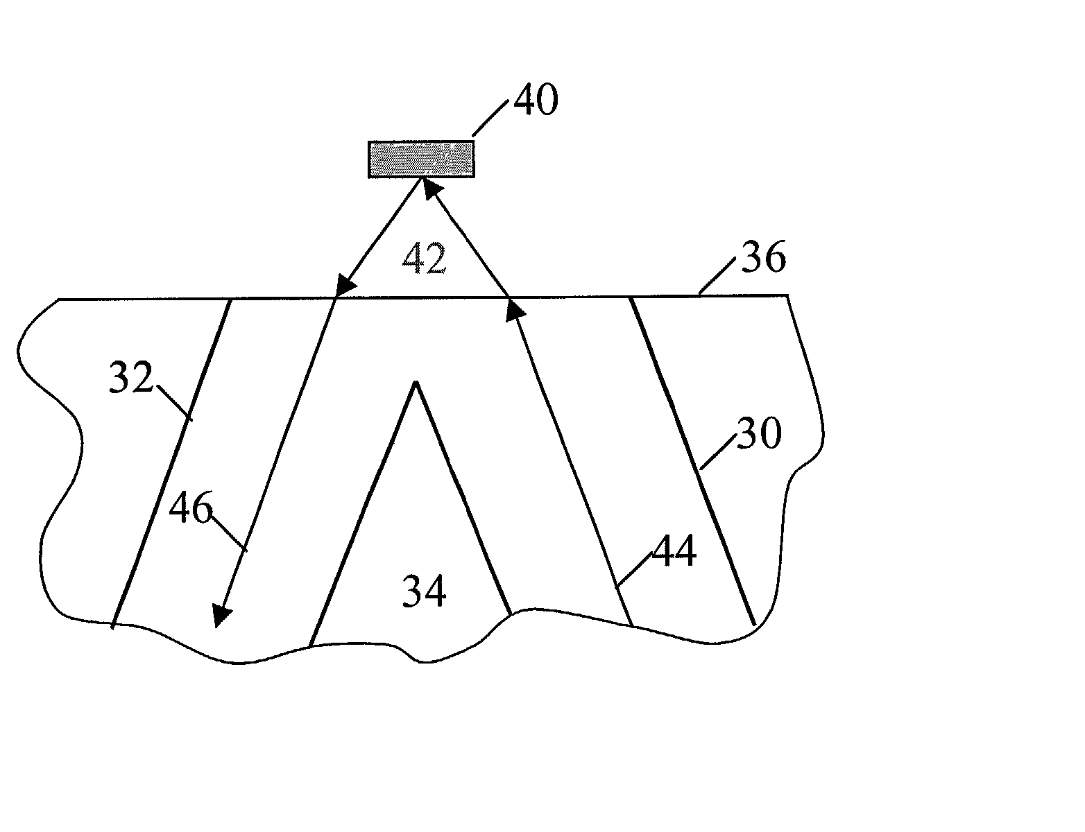
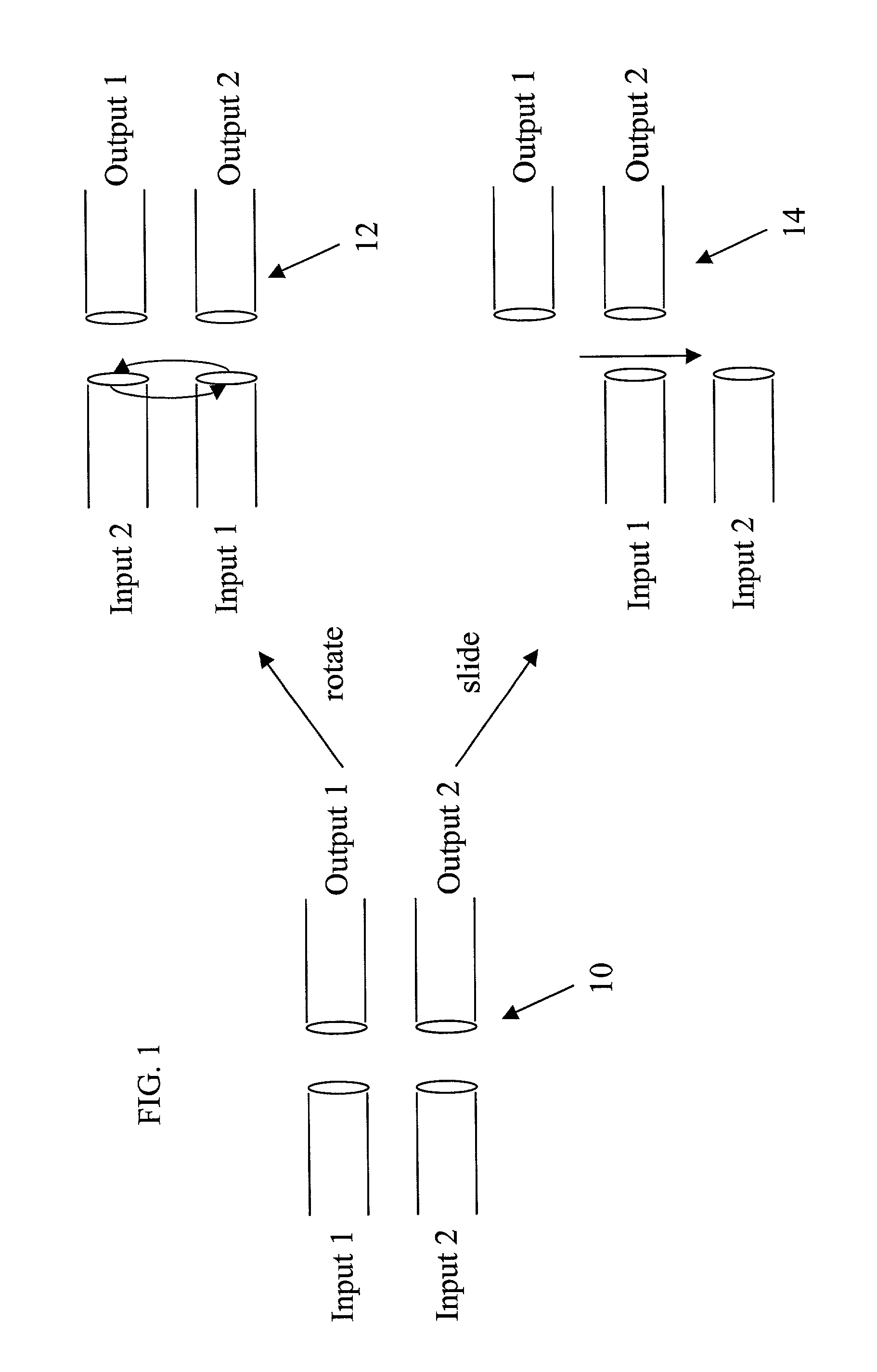
[0012] An aspect of the present invention provides an optical component including a waveguide substrate having an edge and having first and second waveguides formed within the waveguide substrate, the first waveguide having a first end on the edge and the second waveguide having a second end on the same edge. A mirror is positioned adjacent to the edge of the waveguide substrate to receive an optical signal from the first end of the first waveguide and direct the optical signal to the second end of the second waveguide in at least one position of the mirror. The mirror is movable to alter the amount of coupling between the first waveguide and the second waveguide.

[0013] Another aspect of the present invention provides an optical component including a waveguide substrate having an edge and having first, second and third planar waveguides extending within the waveguide substrate, each of the first, second and third waveguides having an optical path extending through the edge of the wa...


PUM


Abstract

An assembly that could be used either as a switch or an attenuator includes two or more optical channels defined by lithography within a substrate. The two or more optical channels are positioned so that the ends of the optical channels are at or near an edge of the substrate. A moveable MEMS mirror is positioned near the edge of the substrate and the openings, with the face of the mirror positioned to receive an optical signal from one of the optical channels. The mirror can direct an optical signal from one of the optical channels into another of the optical channels. Mirror position can be changed to alter the path of the optical signal and to change the coupling between the optical channels. In this way, the assembly of optical channels within the substrate and the MEMS mirror can act as a switch or as an attenuator.

Description

[0001] 1. Field of the Invention[0002] The present invention relates to integrated optical components and, in particular, to optical components capable of switching and / or attenuating at least one optical channel and performing add or drop functions for optical channels. Particularly preferred implementations facilitate switching and / or attenuating arrays of optical channels.[0003] 2. Description of the Related Art[0004] Optical networks are used for wide area and long distance communication, including for the backbone of the Internet. Demand for additional bandwidth in short haul (i.e., metro) and long haul applications continues to grow and a variety of different strategies have been adopted to make optical networks less expensive and more flexible. Optical networks use a variety of components, including add / drop modules, attenuators and optical switches. Generally these components are bulky, expensive and have low levels of integration. The lack of adequate, reliable and cost-eff...

Claims


Application Information

Patent Timeline
IPC IPC(8): G02B6/26G02B6/35
CPCG02B6/266G02B6/3512G02B6/3514G02B6/357G02B6/3588G02B6/3594G02B6/3596
Inventor CHANG, TALLIS Y.LAM, LEOMARTIN, GRAHAM
Owner HEWLETT PACKARD CO
Why Eureka
Try Eureka