Display apparatus and driving method thereof

a display device and drive method technology, applied in the field of active matrix type display devices, can solve the problems of difficult to quickly write the signal current, difficult to achieve the effect of rapid writing of the signal current, and varying the luminance of the el element 3006 among pixels

Inactive Publication Date: 2003-11-20
SEMICON ENERGY LAB CO LTD
View PDF90 Cites 123 Cited by
  • Summary
  • Abstract
  • Description
  • Claims
  • Application Information

AI Technical Summary

Benefits of technology

[0063] In the invention, since the current flowing through the light emitting element on the occasion of carrying out image display is maintained at a predetermined constant current, regardless of change of the current characteristic due to deterioration etc., it is possible to make the light emitting element emit light with constant luminance. Since ON or OFF state of the switch part is selected by the digital video signal and thereby, the light emitting state or the non light emitting state of each pixel is selected, it is possible to quicken the writing of the video signal to the pixel. In the pixel in which the non light emitting state is selected by the video signal, since the current to be inputted to the light emitting element is completely cut off by the switch part, it is possible to express accurate gray scale. In short, it is possible to solve the problem of contrast deterioration due to the leak current on the occasion of black display. Also, in the invention, since it is possible to set the current value of the constant current flowing through the current source circuit large to some extent, it is possible to reduce the influence of noise which occurs on the occasion of writing a small signal current. Further, since a driving circuit for changing current values flowing through the current source circuits disposed in each pixel is not necessary and an external driving circuit fabricated over a separate substrate such as a single crystalline IC substrate etc., it is possible to realize a lower cost and a smaller size.

Problems solved by technology

In short, in the voltage writing type analog system, when the current characteristic of the driving TFT 3004 varies, the drain current varies and therefore, there is a problem that luminance of the EL element 3006 varies among pixels.
As a result, in a display device having a pixel of such a type that the driving TFT is made to be operated in the linear region, burn-in of an image tends to occur.
On that account, it is difficult to quickly write the signal current.
Therefore, there is such a high risk that it is impossible for the pixel to emit light with accurate luminance.
However, in reality, it is hard that the pair of these TFTs have completely the same current characteristics, and there occurs variation.
Even in case that the black display is carried out, there is such a risk that the drain current flows through the driving TFT 2903 and the EL element 2906 emits light, and there occurs a problem that contrast comes down.
However, in a transistor using polycrystalline semiconductors etc., since variation of characteristics of transistors is large, it is difficult to make the video signal input current source in which current characteristics are uniform.
The display device of such structure has such problems that cost is high, and an area of a picture frame can not be reduced since large is an area which is required on the occasion of attachment of the single crystalline IC substrate.
However, only by the above-described method, there is a case that the number of gray scales is not sufficient.

Method used


Image

  • Display apparatus and driving method thereof
  • Display apparatus and driving method thereof
  • Display apparatus and driving method thereof

Examples


embodiment 1

[0109] (Embodiment 1)

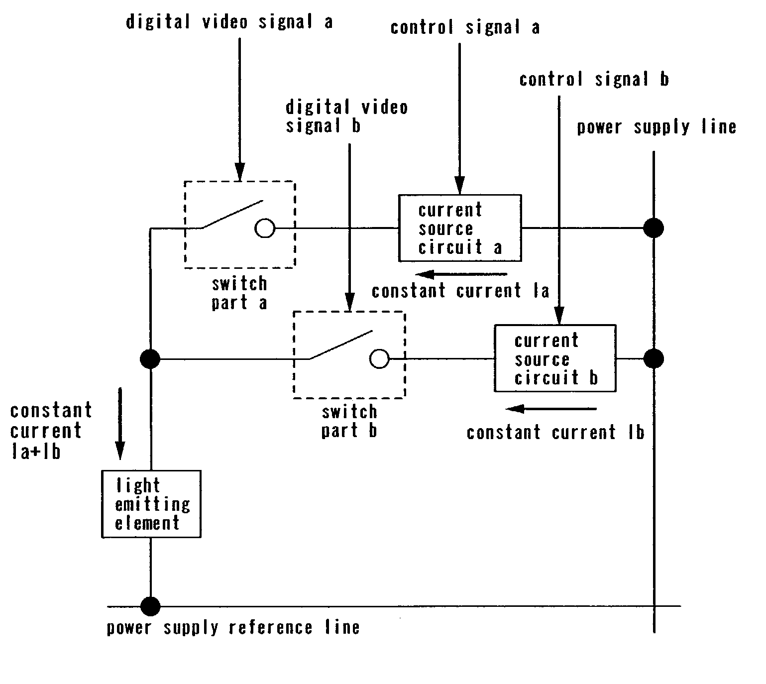
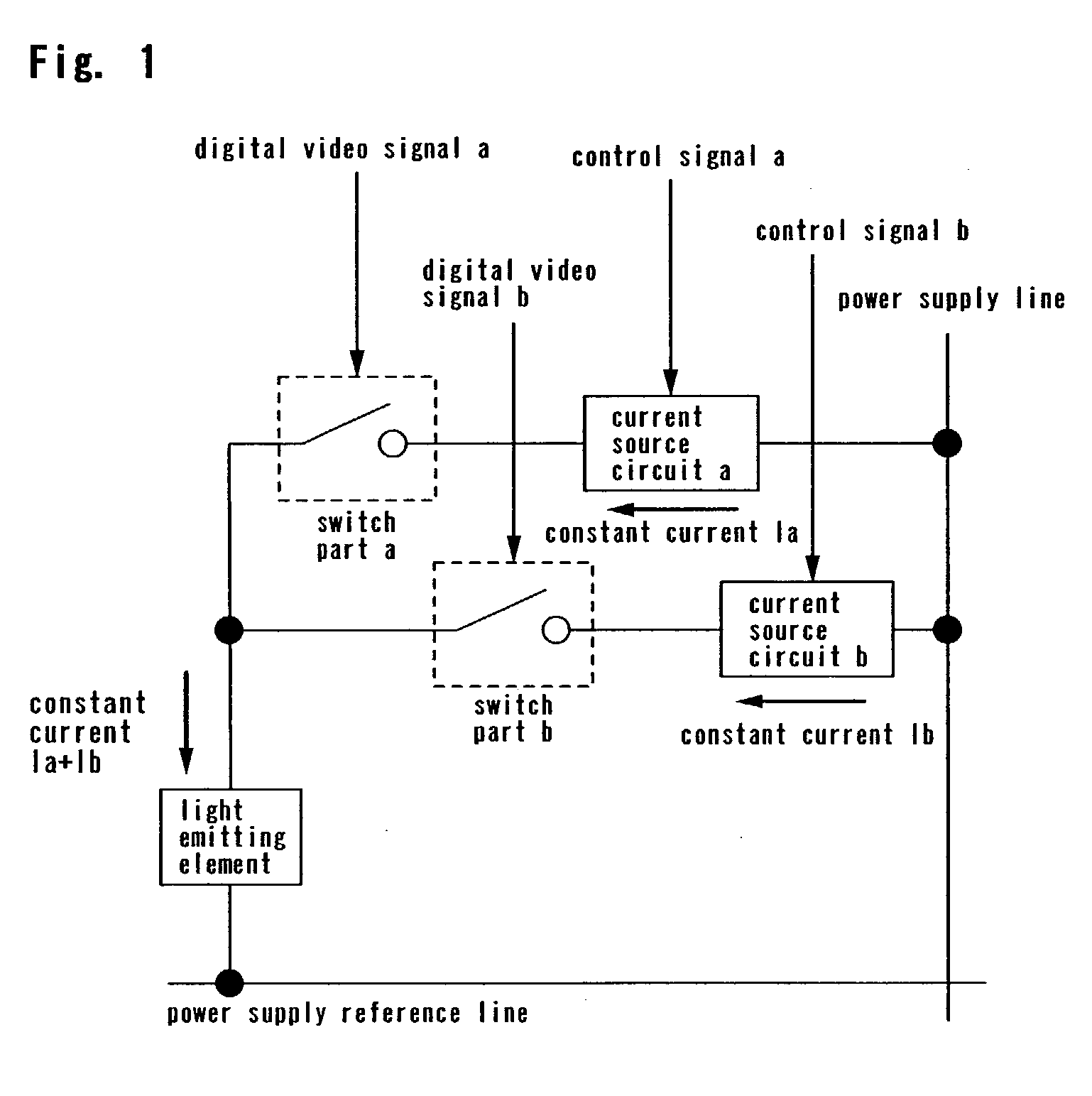
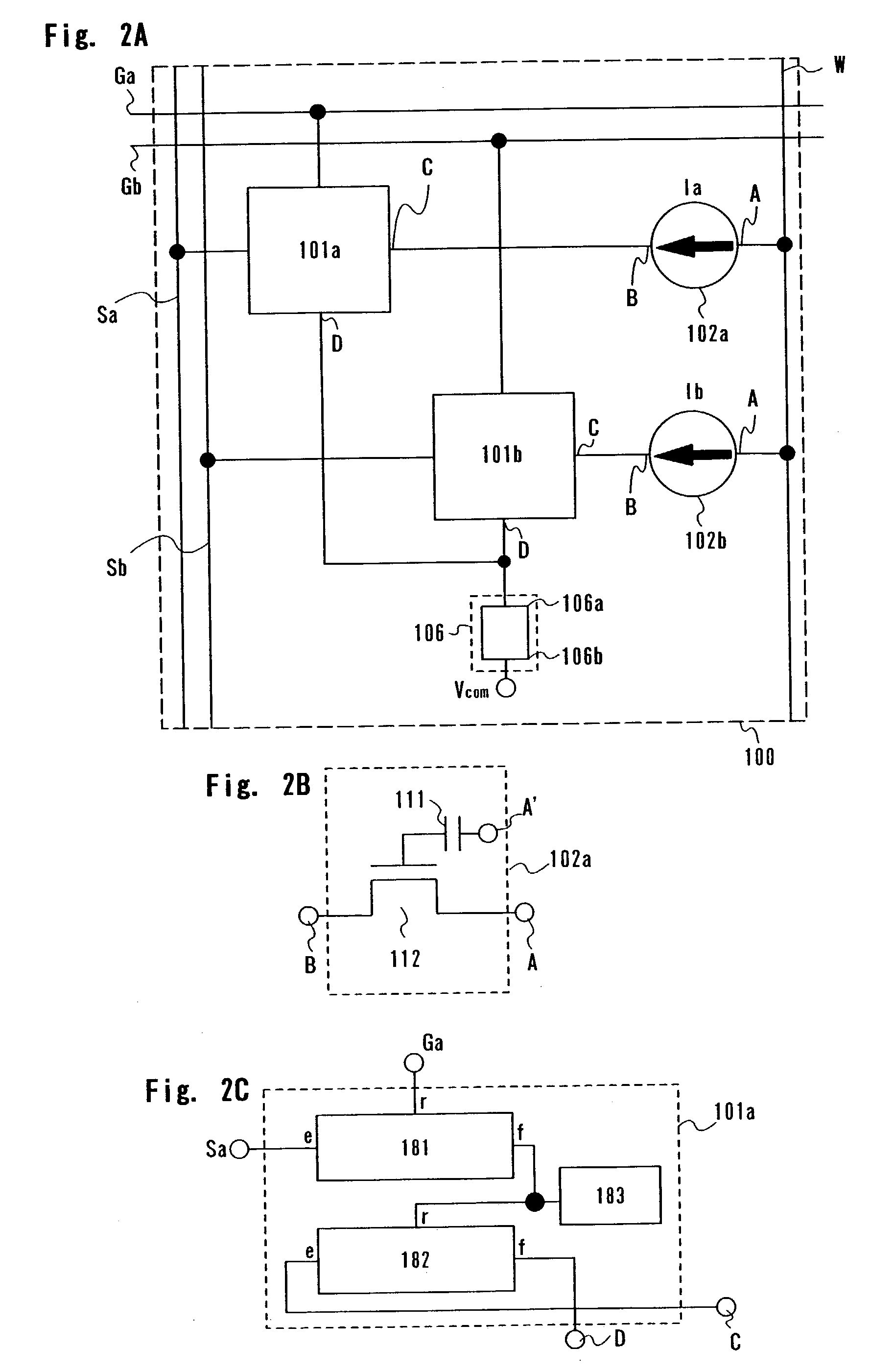
[0110] An embodiment of the invention will be described by use of FIG. 2. In this embodiment, a case that there are two PAIRs in one pixel will be described.

[0111] In FIG. 2A, each pixel 100 has switch parts 101a and 101b, current source circuits 102a and 102b, a light emitting element 106, video signal input lines Sa and Sb, scanning lines Ga and Gb, and a power supply line W. The switch part 101a and the current source circuit 102a are connected serially to form one PAIR. The switch part 102b and the current source circuit 102b are connected serially to form one pair. These two PAIRs are connected in parallel. Also, these two parallel circuits are serially connected to the light emitting element 106.

[0112] In the pixel shown in FIGS. 2A to 2C, two PAIRs are disposed but, hereinafter, paying attention to the PAIR of the switch part 101a and the current source circuit 102a, a structure of the current source circuit 102a and the switch part 101a will be described...

embodiment 2

[0133] (Embodiment 2)

[0134] This embodiment shows a concrete structural example of the switch part of each PAIR included in a pixel in the display device of the invention. Also, an operation of the pixel which has the switch part will be described.

[0135] A structural example of the switch part is shown in FIG. 3. A switch part 101 has a switching transistor 301, a driving transistor 302, a deleting transistor 304, and a holding capacitor 303. In addition, it is possible to omit the holding capacitor 303 by using a gate capacitance etc. of the driving transistor 302. A transistor which configures the switch part 101 may be a single crystalline transistor, or a polycrystalline transistor, or an amorphous transistor. Also, it may be a SOI transistor. It may be a bipolar transistor. It may be a transistor using an organic material, for example, a carbon nanotube.

[0136] A gate electrode of the switching transistor 301 is connected to a scanning line G. One of a source terminal and a drai...

embodiment 3

[0165] (Embodiment 3)

[0166] In this embodiment, a structure and an operation of the current source circuit included in each pixel of the display device of the invention will be described in detail.

[0167] The current source circuit of one PAIR out of a plurality of PAIRs included in each pixel will be watched, and a structure thereof will be described in detail. In this embodiment, although five structural examples of the current source circuit will be cited, another structural example may be fine if it is a circuit which operates as a current source. In addition, a transistor which configures the current source circuit may be a single crystalline transistor, a polycrystalline transistor, or an amorphous transistor. Also, it may be a SOI transistor. It may be a bi-polar transistor. It may be a transistor using an organic material, for example, a carbon nanotube.

[0168] Firstly, a current source circuit of a first structure will be described by use of FIG. 9A. In addition, in FIG. 9A, ...


PUM


Abstract

This invention provides a display device in which it is possible to have a light emitting element emitted light with constant luminance without coming under the influence of deterioration over time, and it is possible to realize accurate gray scale express, and yet, it is possible to speed up writing of a signal current to each pixel, and influence of noise of a leak current etc. is suppressed, and a driving method thereof. A plurality of pairs of switch parts and current source circuits are disposed in each pixel. Switching of each of a plurality of the switch parts is controlled by a digital video signal. When the switch part is turned ON, by a current supplied from the current source circuit making a pair with the switch part, the light emitting element emits light. A current which is supplied from one current source circuit to the light emitting element is constant. A value of a current flowing through the light emitting element is comparable to a value of added currents which are supplied to the light emitting element from respective all current source circuits making pairs with the switch parts which are in the conductive states.

Description

[0001] 1. Field of the Invention[0002] This invention relates to a display device using a light emitting element and a driving method thereof. More particularly, it relates to an active matrix type display device in which a light emitting element is disposed in each pixel and a transistor for controlling light emission of the light emitting element is provided and a driving method thereof.[0003] 2. Description of the Related Art[0004] Development of a display device having a light emitting element has been put forward in these years. In particular, development of an active matrix type display device in which a light emitting element and a transistor for controlling light emission of the light emitting element are disposed in each pixel has been put forward.[0005] In the active matrix type display device, either a technique in which an input of luminance information to each pixel is carried out by a voltage signal or a technique in which it is carried out by a current signal is mainl...

Claims


Application Information

Patent Timeline
Patent Type & Authority Applications(United States)
IPC IPC(8): G09G3/20G09G3/32
CPCG09G3/2022G09G2360/18G09G3/2081G09G3/3233G09G3/3241G09G3/3266G09G3/3283G09G2300/0809G09G2300/0828G09G2300/0842G09G2300/0852G09G2300/0861G09G2300/0866G09G2310/0216G09G2310/0251G09G2310/0262G09G2310/061G09G2320/0252G09G2320/043G09G3/2077G09G3/30
Inventor KIMURA, HAJIME
Owner SEMICON ENERGY LAB CO LTD
Why Eureka
Try Eureka