Substrate identification circuit and semiconductor device

a technology of identification circuit and substrate, applied in the direction of identification means, instruments, optics, etc., can solve the problems of increasing cost, time and effort, and difficulty in selectively giving a right to the tft substrate, and achieving the effect of reducing the number of chips, and improving the number of chips

Inactive Publication Date: 2003-11-27
SEMICON ENERGY LAB CO LTD
View PDF4 Cites 11 Cited by
  • Summary
  • Abstract
  • Description
  • Claims
  • Application Information

AI Technical Summary

Problems solved by technology

First, the usage of a component separated from the TFT substrate for the sake of giving an identification number is not preferable because this leads to an increase in cost, time, and effort.
If it is possible to rewrite the substrate identification number on the TFT substrate without difficulty, for instance, it becomes difficult to selectively give a right to the TFT substrate.
At the same time, it becomes possible to realize a substrate identification circuit that achieves a high level of safety by making it difficult to rewrite or duplicate a substrate identification number.
In reality, however, all of TFTs produced on an insulating substrate exhibit variations in their characteristics, so that there occurs a problem to be described below in the case where the substrate identification circuit described above that uses the aforementioned scheme is realized as it is.
In addition, it is difficult to rewrite or duplicate the proper number.
Also, in the case where the TFT size is far smaller than the typical grain size, most TFTs are formed by a single grain, although grain boundaries exist in the channel regions of some TFTs and therefore their characteristics greatly vary and exhibit unbalanced characteristic variations.
However, in the case where the number of stages of the inverters or buffer circuits is small, there is a possibility that the output potential is not sufficiently shifted to the Hi or Lo side and becomes an intermediate potential.

Method used


Image

  • Substrate identification circuit and semiconductor device
  • Substrate identification circuit and semiconductor device
  • Substrate identification circuit and semiconductor device

Examples


first embodiment

[0107] [First Embodiment]

[0108] In this embodiment, there will be described a concrete circuit construction of the proper bit generating circuit described in the embodiment mode. The following description will be made with reference to FIG. 6.

[0109] The proper bit generating circuit shown in FIG. 6 receives input of potentials Vin1 and Vin2 and outputs a proper bit Did. In FIG. 6, the drain region of an N-channel type TFT 602 and the drain region of a P-channel type TFT 604 are connected to each other at a node A, while the drain region of the N-channel type TFT 603 and the drain region of the P-channel type TFT 605 are connected to each other at a node B. The source region of the N-channel type TFT 602 and the source region of the N-channel type TFT 603 are connected to each other and are connected to a constant current source. The source region of the P-channel type TFT 604 and the source region of the P-channel type TFT 605 are connected to each other and are connected to a power...

second embodiment

[0116] [Second Embodiment]

[0117] In this embodiment, as a concrete circuit construction of the proper bit generating circuit, there will be described an example that is different from that in the first embodiment. The following description will be made with reference to, FIG. 7.

[0118] The proper bit generating circuit shown in FIG. 7 receives input of potentials Vin1 and Vin2 and outputs a proper bit Did. In FIG. 7, the drain region of an N-channel type TFT 701 and the drain region of a P-channel type TFT 702 are connected to each other at a node C. The node C is connected to the input terminal of an inverter 703 and this inverter 703 is connected to another inverter 704 in series. The inputs Vin1 and Vin2 into the proper bit generating circuit are respectively connected to the gate electrode of the P-channel type TFT 702 and the gate electrode of the N-channel type TFT 701, and the proper bit Did that is an output from the proper bit generating circuit is connected to the output te...

third embodiment

[0125] [Third Embodiment]

[0126] In this embodiment, as a concrete circuit construction of the proper word generating circuit, there will be described an example that is different from that in the embodiment mode. The following description will be made with reference to FIG. 8.

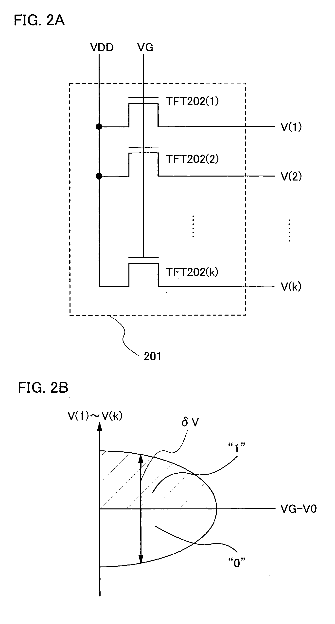
[0127] In FIG. 8, there is shown a proper word generating circuit that receives input of potentials Vin1 and Vin2 and outputs a k-bit (k is an integer at least equal to one) proper word (Did(1), . . . , Did)k). The proper word generating circuit shown in FIG. 8 is constructed from a reference voltage generating circuit 802 and k proper bit generating circuits 801(1) to 801(k). The k proper bit generating circuits 801(1) to 801(k) are each constructed from a pair of an N-channel type TFT and a P-channel type TFT [805(1), 806(1)] to [805(k), 806(k)], and the circuit construction thereof is identical to the construction shown in FIG. 7 from which the inverters 703 and 704 are removed. Also, the operation thereof i...


PUM

PropertyMeasurementUnit
temperatureaaaaaaaaaa
thicknessaaaaaaaaaa
thicknessaaaaaaaaaa

Abstract

Provided is a substrate identification circuit that generates a numeric value, whose duplication is difficult and which is proper to a substrate, at low cost and a semiconductor device having such a substrate identification circuit. A substrate identification circuit 304 is produced by utilizing variations in characteristics among TFTs formed on a substrate having an insulating surface. The substrate identification circuit 304 includes a plurality of proper bit generating circuits, each of which is constructed from a plurality of TFTs and outputs a one-bit random number based on variations in characteristics among the plurality of TFTs. The substrate identification circuit generates a numeric value proper to the substrate using the one-bit random number. The substrate identification circuit may include a circuit that makes a judgment by comparing the numeric value proper to the substrate with an identification number inputted from the outside.

Description

[0001] 1. Field of the Invention.[0002] The present invention relates to a substrate identification circuit constructed from a thin film transistor formed on a substrate having an insulating surface, and a semiconductor device.[0003] 2. Description of the Related Art.[0004] In recent years, semiconductor devices, particularly electric equipment with semiconductor display portions have made remarkable developments. There are variety of application examples thereof, including game machines, notebook computers, portable equipment represented by mobile telephones, liquid crystal televisions, liquid crystal displays, electro-luminescent (EL) displays and the like. Compared to conventional cathode ray tubes (CRT), it is possible to form thinner lightweight displays for semiconductor display portions featuring low energy consumption.[0005] Semiconductor display portions are classified into two types, a passive matrix type and an active matrix type, but in recent years especially, technolog...

Claims


Application Information

Patent Timeline
Patent Type & Authority Applications(United States)
IPC IPC(8): G02F1/1368G09F9/00G09F9/30G09F9/35H01L21/02H01L21/77H01L21/84H01L23/544H01L27/12H01L29/786
CPCH01L23/544H01L27/12H01L27/1214H01L2223/54433H01L2223/5444H01L2924/0002H01L2924/12044H01L2924/00
Inventor KATO, KIYOSHIYAMAZAKI, SHUNPEI
Owner SEMICON ENERGY LAB CO LTD
Why Eureka
Try Eureka