Test method for yielding a known good die

a test method and die technology, applied in the direction of individual semiconductor device testing, semiconductor/solid-state device testing/measurement, instruments, etc., can solve the problems of increasing the cost of testing at the wafer level, wasting burn-in resources on dice, and packaging more defective di

Inactive Publication Date: 2003-12-25
FORMFACTOR INC
View PDF53 Cites 66 Cited by
  • Summary
  • Abstract
  • Description
  • Claims
  • Application Information

AI Technical Summary

Problems solved by technology

But in doing so they encounter the added costs of packaging more defective dice or expending burn-in resources on dice that could have been classified as defective before they were subjected to burn-in.
Since a wafer level IC tester must include a separate data input / output channel to communicate with each IC pad it accesses during a test, tests carried out at the wafer level are often limited to those requiring a tester to access only a relatively few pads on each IC.
However since a single defective dice renders the entire FCM defective, many manufacturers find it preferable to test singulated dice before they are incorporated into FCMs.
However the need to separately handle each IC chip during the many processing steps occurring after singulation increases the cost and lowers the speed of the process.
Since the dice on a single wafer can collectively have a very large number of signal pads, it is usually not practical to provide a tester having a sufficient number of channels to access all of the signal pads concurrently.
But the process flow of FIG. 3 has an inherent inefficiency not shared by the process flow of FIG. 2.
The process flow of FIG. 3 may conduct analogous test and burn-in steps on the wafer level dice, but since the dice are not singulated until after all testing and burn-in steps are complete, it is not possible to discard dice found to be defective after each test.
Such redundant testing of known defective dice is an inefficient use of test and burn-in resources and can be particularly problematic where dice yields are low.

Method used


Image

  • Test method for yielding a known good die
  • Test method for yielding a known good die
  • Test method for yielding a known good die

Examples


Embodiment Construction

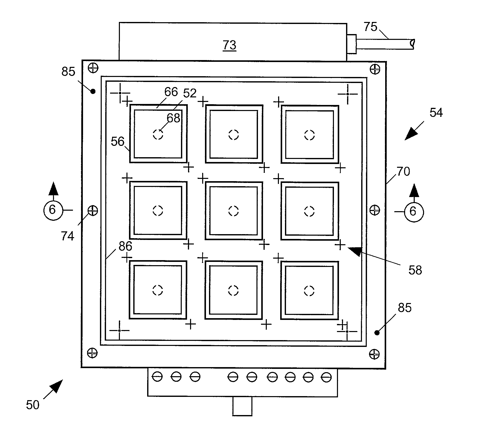
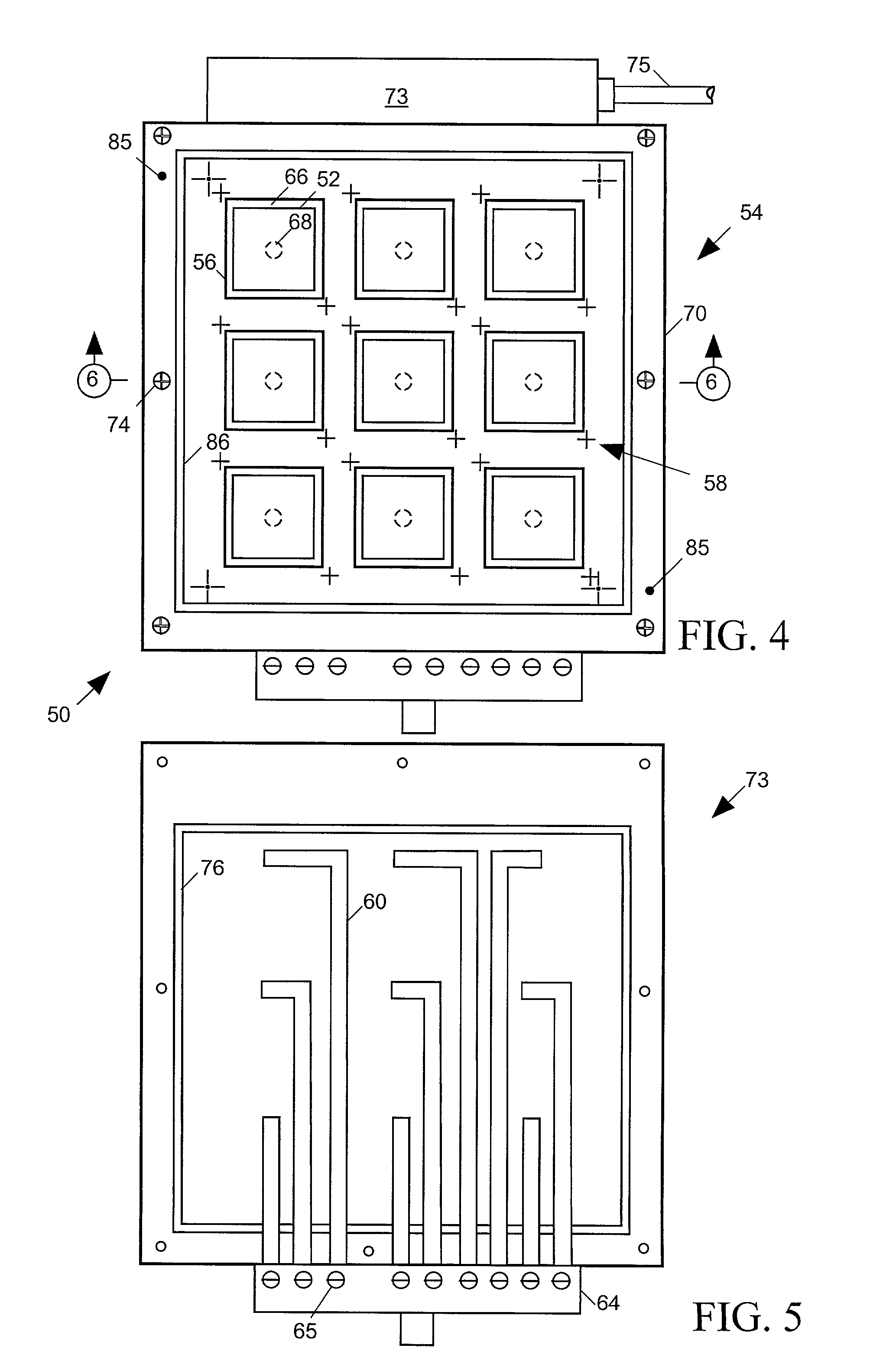
[0038] The present invention relates to a system for testing and processing an array of singulated integrated circuit (IC) dice held on a carrier, and this specification describes one or more exemplary embodiments and applications of the invention considered by the applicants to be the best modes of practicing the invention. It is not intended, however, that the invention be limited to the exemplary embodiments described below or to the manner in which the embodiments operate.

[0039] FIG. 4 is a top plan view of a silicon panel carrier 50 in accordance with an exemplary embodiment of the invention, and FIGS. 5 and 6 are sectional plan and elevation views, respectively, of the carrier of FIG. 4. Carrier 50 includes a base 54 having a 3.times.3 array of recesses 56, each having an upper opening and a planar bottom for holding a separate one of IC dice 52. While for simplicity, carrier 50 of FIGS. 4-6 is illustrated as having a 3.times.3 array of recesses 56, in other embodiments of the...


PUM


Abstract

A semiconductor wafer is cut to singulate integrated circuit dice formed on the wafer. A die pick machine then positions and orients the singulated dice on a carrier base such that signal, power and ground pads formed on the surface of each die reside at predetermined positions relative to landmarks on the carrier base the die pick machine optically identifies. With the dice temporarily held in place on the carrier base, they are subjected to a series of testing and other processing steps. Since each die's signal pads reside in predetermined locations, they can be accessed by appropriately arranged probes providing test equipment with signal access to the pads during tests. After each test, a die pick machine may replace any die that fails the test with another die, thereby improving efficiency of subsequent testing and other processing resources.

Description

[0001] 1. Field of the Invention[0002] The present invention relates in general to integrated circuit (IC) fabrication and testing processes and in particular to the use of a carrier for holding an array of IC dice during testing and other processing steps.[0003] 2. Description of Related Art[0004] FIG. 1 illustrates a typical prior art process flow for fabricating, packaging and testing ICs having embedded repairable random access memories (RAMs). A RAM includes rows and columns of cells for storing data, and a laser-repairable RAM includes spare rows or columns that can be used to replace rows or columns containing defective cells. When an IC chip containing a laser-repairable memory has a defective row or column, a laser alters the IC chip by cutting selected fuses on the surface of the IC so that the IC uses a spare row or column in lieu of the defective row or column.[0005] In the process flow depicted in FIG. 1, the ICs are initially fabricated as an array of IC dice on a semi...

Claims


Application Information

Patent Timeline
Patent Type & Authority Applications(United States)
IPC IPC(8): G01R31/28G11C29/00G01R1/06G11C29/56
CPCG01R31/2831G01R31/2886G11C29/56016G11C29/006G11C29/56G01R31/31718H01L22/00
Inventor MILLER, CHARLES A.COOPER, TIMOTHYHATSUKANO, YOSHIKAZU
Owner FORMFACTOR INC
Why Eureka
Try Eureka