Stacked wafer aligment method

Inactive Publication Date: 2004-02-05
TORAY ENG CO LTD
View PDF3 Cites 18 Cited by
  • Summary
  • Abstract
  • Description
  • Claims
  • Application Information

AI Technical Summary

Problems solved by technology

In such a condition, it is difficult to precisely read the recognition mark to be read, and a high-accuracy alignme

Method used


Image

  • Stacked wafer aligment method
  • Stacked wafer aligment method
  • Stacked wafer aligment method

Examples


Embodiment Construction

[0016] Hereinafter, desirable embodiments of the present invention will be explained referring to figures.

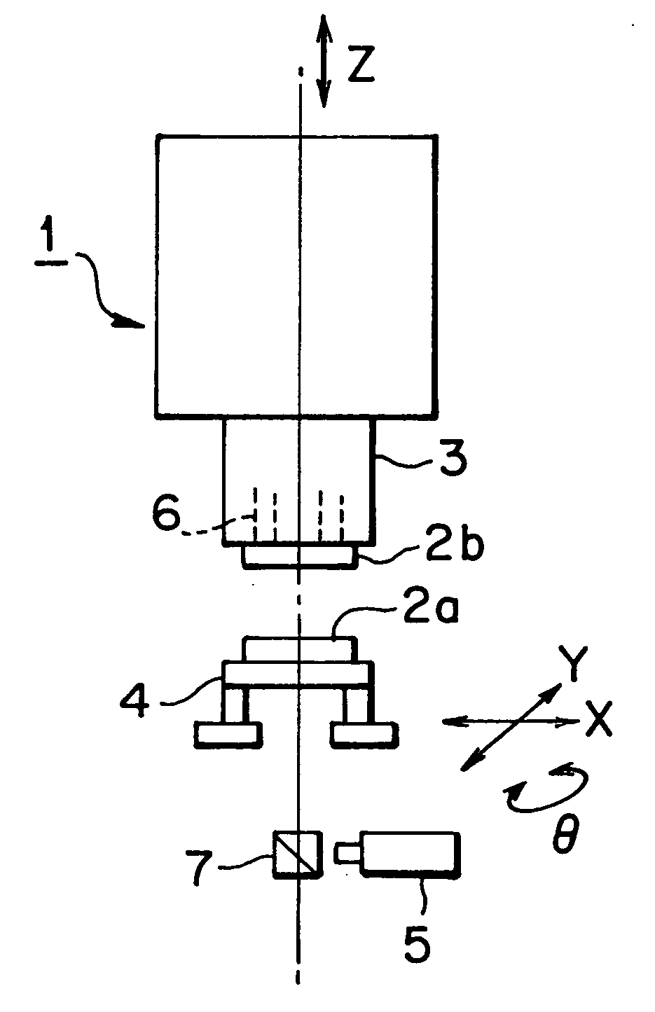
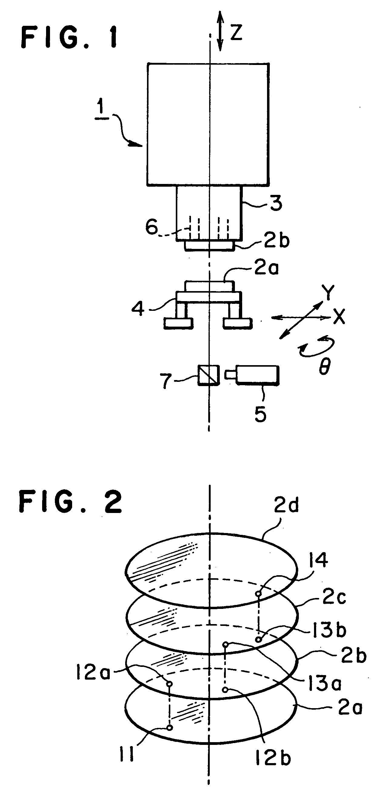
[0017] FIG. 1 shows a schematic structure of a mounting device bonding wafers for carrying out a stacked wafer alignment method according to an embodiment of the present invention. FIG. 2 shows a state for stacking wafers in order.

[0018] In FIG. 1, label 1 shows the whole of a mounting device, and labels 2a and 2b show wafers to be stacked and bonded. Although only two wafers 2a and 2b are shown in FIG. 1, in practice, as shown in FIG. 2, three or more wafers 2a, 2b, 2c, . . . are stacked in order.

[0019] In this embodiment, an upper-side wafer 2b to be stacked, shown in FIG. 1, is held on a head 3 by, for example, an electrostatic chuck and the like, and the head 3 can be moved in Z direction (vertical direction). A lower-side wafer 2a is held on a stage 4 by an electrostatic chuck and the like. In this embodiment, this stage 4 can be adjusted in position in X and Y directions (...


PUM


Abstract

A stacked wafer alignment method with ease and with high precision in which a recognition mark for alignment is provided on each wafer, three or more wafers are stacked while adjacent two wafers are aligned with each other and the positions of the recognition marks of the wafers are shifted in the circumferential direction from one another in order.

Description

Technical Field of the Invention The present invention relates to an alignment method for positioning adjacent wafers when three or more wafers are stacked.[0001] Background Art of the Invention[0002] For example, in a mounting device for bonding wafers, an aligner for aligning a wafer at a predetermined position in order to process the wafer or to mount a chip or other parts on the wafer, or an exposure device for providing a predetermined exposure to a wafer, it may be required to stack a plurality of wafers, particularly, three or more wafers, in order, and to form a compact stacked body of the plurality of wafers.[0003] To satisfy such a requirement, a wafer to be stacked must be aligned at a high accuracy relative to a lower wafer. In the conventional technology, for example, when two wafers are aligned with each other, a recognition mark for alignment has been provided on each wafer and a desired-accuracy alignment is carried out by aligning the positions of the recognition ma...

Claims


Application Information

Patent Timeline
IPC IPC(8): G03F9/00H01L21/00H01L21/027H01L21/68H01L21/98H01L23/544H01L25/065H01L25/07H01L25/18
CPCH01L21/67253H01L21/67294H01L21/681H01L21/682H01L23/544H01L25/50H01L2924/0002H01L2223/54453H01L2225/06593H01L2924/00H01L21/68
Inventor YAMAUCHI, AKIRA
Owner TORAY ENG CO LTD
Why Eureka
Try Eureka