Switching element and method of making the same

a technology of switching element and film, applied in the field of switching element, can solve the problems of low film uniformity, unknown switching mechanism, and concomitant trend of increasing component density

Inactive Publication Date: 2004-06-10
ROHM CO LTD
View PDF5 Cites 10 Cited by
  • Summary
  • Abstract
  • Description
  • Claims
  • Application Information

AI Technical Summary

Problems solved by technology

In recent years, with ongoing miniaturization of electronic devices, there is a concomitant trend of increasing density in components.
However, the switching mechanism is not yet known.
The Cu-TCNQ film made in the solution spreading method is a polycrystalline film formed of relatively large crystals, and therefore is low in film uniformity.
This non-uniformity in the film causes various problems.
Another problem is that the Cu-TCNQ film is poor in stability.
Because of these problems, no market has ever seen electronic devices incorporating a switching element provided by a conventional Cu-TCNQ film formed by means of the solution spreading method.
Another problem is that according to the solution spreading method it is difficult to control the thickness of the growing film.
However, in such a method of control on the film thickness, it is difficult to obtain a desired thickness of the film.

Method used


Image

  • Switching element and method of making the same
  • Switching element and method of making the same
  • Switching element and method of making the same

Examples


embodiment 1

[0090] [Embodiment 1]

[0091]

[0092] A glass substrate (10.times.10.times.1 mm; manufactured by Matsunami Glass Ind., Ltd,) on which an ITO layer (300 nm thickness) was formed in advance, was mounted to a copper substrate specifically made for a vapor depositing apparatus (Vapor Depositing Apparatus E100 for Organic EL Research and Development; manufactured by Advanced Lab Systems Co., Ltd), and then set to a substrate holder in the chamber of the apparatus. A tungsten spiral boat loaded with approximately 1 gram of Al (manufactured by Nilaco Corporation) was connected to the electrode in the chamber. Next, pressure inside the chamber was reduced, and under the vacuum range between 3 to 4.times.10.sup.-3 Pa, Al was vaporized and deposited on the substrate. The depositing rate was 1 to 1.5 .ANG. / sec and the deposition was continued to a thickness of 20 nm. Thereafter, the pressure in the chamber was returned to the normal atmospheric pressure, and using a UV ozone cleaner (manufactured...

embodiments 2 and 3

[0101] [Embodiments 2 and 3]

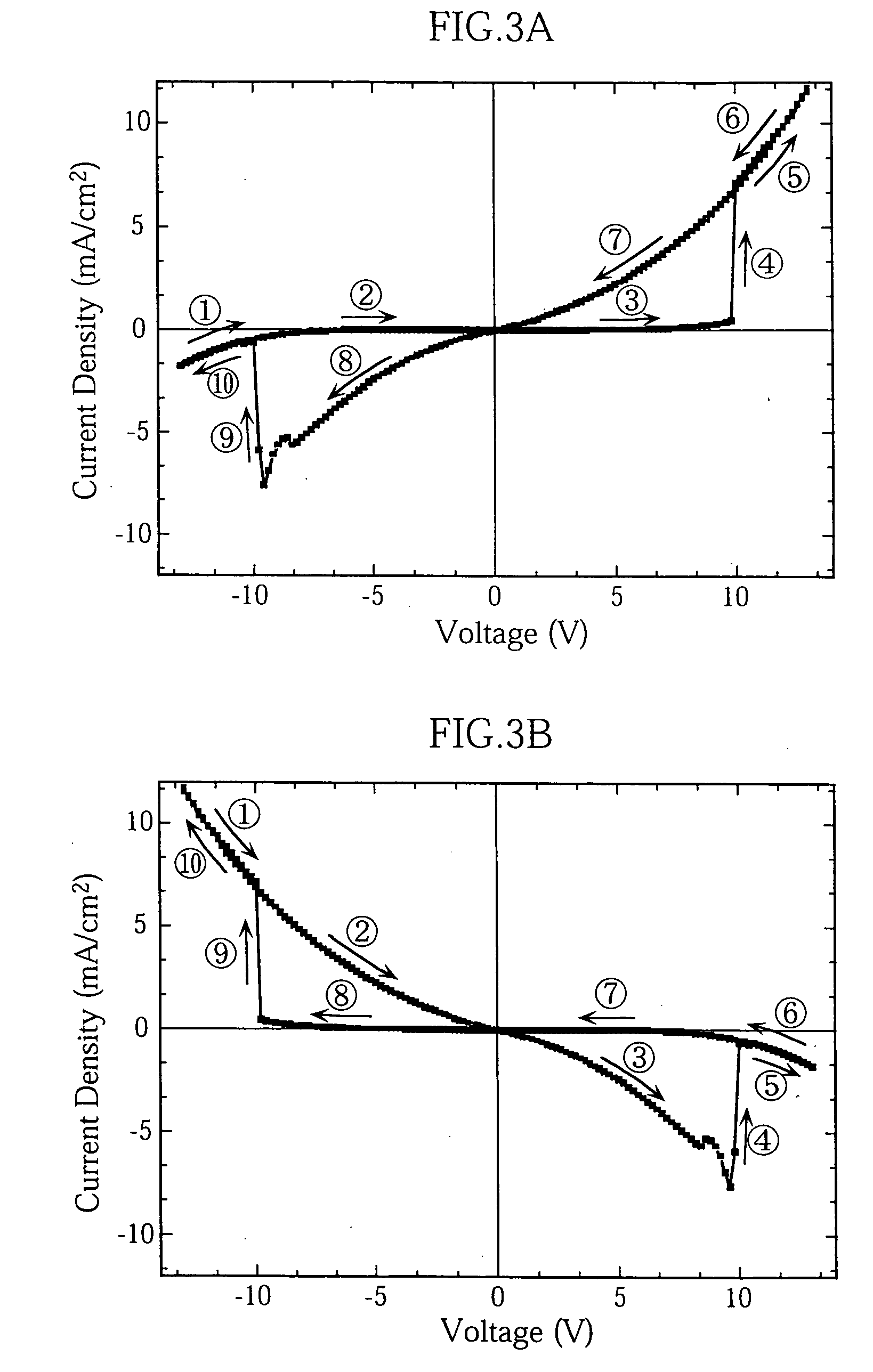
[0102] Switching elements were made in the same way as in Embodiment 1, except that the Cu and TCNQ deposition ratio was changed to 1:2 (for Embodiment 2) and 3:2 (for Embodiment 3). The element structures of Embodiments 2 and 3 are given in FIG. 12. These switching elements were also subjected to the same aging process and the J-V measurement as was Embodiment 1, and J-V characteristic curves showing a similar switching characteristic to that of Embodiment 1 were obtained. These switching functions were reproducible over 100 cycles.

[0103] [Reference 1]

[0104] A switching element was made in the same way as in Embodiment 1, except that the Cu and TCNQ deposition ratio was changed to 0:1. The element structure of this reference is given in FIG. 12. The switching element was also subjected to the same aging process and the J-V measurement as was Embodiment 1. No switching function was observed. A J-V characteristic curve obtained for this reference is shown ...

embodiments 4 through 6

[0107] [Embodiments 4 through 6]

[0108] Switching elements were made in the same way as in Embodiment 1, except that the thickness of the switching layer (Cu-TCNQ thin film) was changed to 50 nm (for Embodiment 4), 200 nm (for Embodiment 5), and 300 nm (for Embodiment 6). The element structures of Embodiments 4 through 6 are given in FIG. 12. These switching elements were also subjected to the same aging process and the J-V measurement as was Embodiment 1, and J-V characteristic curves showing a similar switching characteristic to that of Embodiment 1 were obtained. These switching functions were reproducible over 100 cycles.


PUM


Abstract

The switching element has a switching layer between a first electrode layer and a second electrode layer. The switching layer includes a charge transfer complex containing an electron donor and an electron acceptor. An insulating layer is provided between the first electrode layer and the switching layer, and contacts the switching layer. The switching layer switches from a high-resistance state to a low-resistance state upon application of a voltage greater than a first threshold value in a first bias direction. Thereafter, the switching layer maintains the low-resistance state when the applied voltage decreases beyond the first threshold value. When the applied voltage becomes not smaller than a second threshold value in a second bias direction or a reverse direction to the first bias direction, the switching layer switches from the low-resistance state to the high-resistance state. Thereafter, the switching layer maintains the high-resistance state when the applied voltage decreases beyond the second threshold value.

Description

[0001] 1. Field of the Invention[0002] The present invention relates to a switching element which operates in response to a change in applied voltage.[0003] 2. Description of Related Art[0004] Electric conductivity in some materials changes drastically when an applied voltage changes. One of such materials is Cu-TCNQ, a copper complex of 7,7,8,8-tetracyanoquinonedimethane or TCNQ. Cu-TCNQ is a charge transfer complex including copper which serves as an electron donor and TCNQ which serves as an electron acceptor. When a voltage applied to the Cu-TCNQ is swept from a low-voltage side to a high-voltage side, the value of current increases drastically at a certain threshold voltage. Such a switching characteristic of the Cu-TCQN is disclosed in the article "Electrical switching and memory phenomena in Cu-TCNQ thin films" (R. S. Potember et al., Applied Physics Letter 34(6), pp. 405-407, Mar. 15, 1979).[0005] The switching characteristic of Cu-TCNQ is expected to be utilized in a wide r...

Claims


Application Information

Patent Timeline
Patent Type & Authority Applications(United States)
IPC IPC(8): H01L27/28H01L49/02H01L51/05H01L51/30H01L51/40
CPCH01L27/28H01L51/0084H01L51/0051H10K19/00H10K85/611H10K85/341
Inventor TANAKA, HARUOADACHI, CHIHAYAOYAMADA, TAKAHITOSASABE, HIROYUKI
Owner ROHM CO LTD
Why Eureka
Try Eureka