Display substrate, electro-optical device, and electronic apparatus

a technology of electro-optical devices and substrates, applied in the direction of static indicating devices, identification means, instruments, etc., can solve the problems of deterioration in display quality, uneven brightness, and deterioration of display quality of electro-optical devices

Active Publication Date: 2004-06-10
SEIKO EPSON CORP
View PDF3 Cites 34 Cited by
  • Summary
  • Abstract
  • Description
  • Claims
  • Application Information

AI Technical Summary

Problems solved by technology

First, as illustrated in FIG. 18, in order to arrange the conductive portion 103a in the third region 101c, the third region 101c of the frame portion 101 becomes wider by the width W.sub.1 of the conductive portion 103a. It is preferable that the frame portion 101 formed at the periphery of the matrix display portion 100 be as narrow as possible for purposes of miniaturization.
Second, as illustrated in FIG. 18, in the case where the position of the connection between the mounting terminal portion 102 and the conductive portion 103a, that is, the feeding point of the corresponding electro-optical device is made point A, the position where the power source line 104 X.sub.1 closest to the conductive portion 103a is connected to the supply portion 103b is made point B, and the position where the power source line 104 X.sub.n remotest from the conductive portion 103a is connected to the supply portion 103b is made point C, electric potentials in the respective points A, B, and C are indicated as V.sub.A, V.sub.B, and V.sub.C, voltage drops by V1 at the point C separated from the point B by the distance L.sub.1 ,as illustrated in FIG. 19. For simplification, the graph of FIG. 19 illustrates a construction wherein almost constant current is supplied to all of the current-drive elements.
In the case where the current-drive element is a light emitting element, the voltage drop causes brightness unevenness.
Thus, the display quality of the electro-optical device deteriorates.
Thus, unevenness in dynamic current supply and brightness unevenness is caused by the dynamic voltage variation, and deterioration in the display quality results.
This voltage drop causes brightness unevenness in a vertical direction, and thereby deteriorates the display quality of the electro-optical device.
Thus, unevenness in the dynamic current supply and the. brightness unevenness is caused by the dynamic voltage variation, and deterioration in the display quality results.

Method used


Image

  • Display substrate, electro-optical device, and electronic apparatus
  • Display substrate, electro-optical device, and electronic apparatus
  • Display substrate, electro-optical device, and electronic apparatus

Examples


first embodiment

of Electro-optical Device

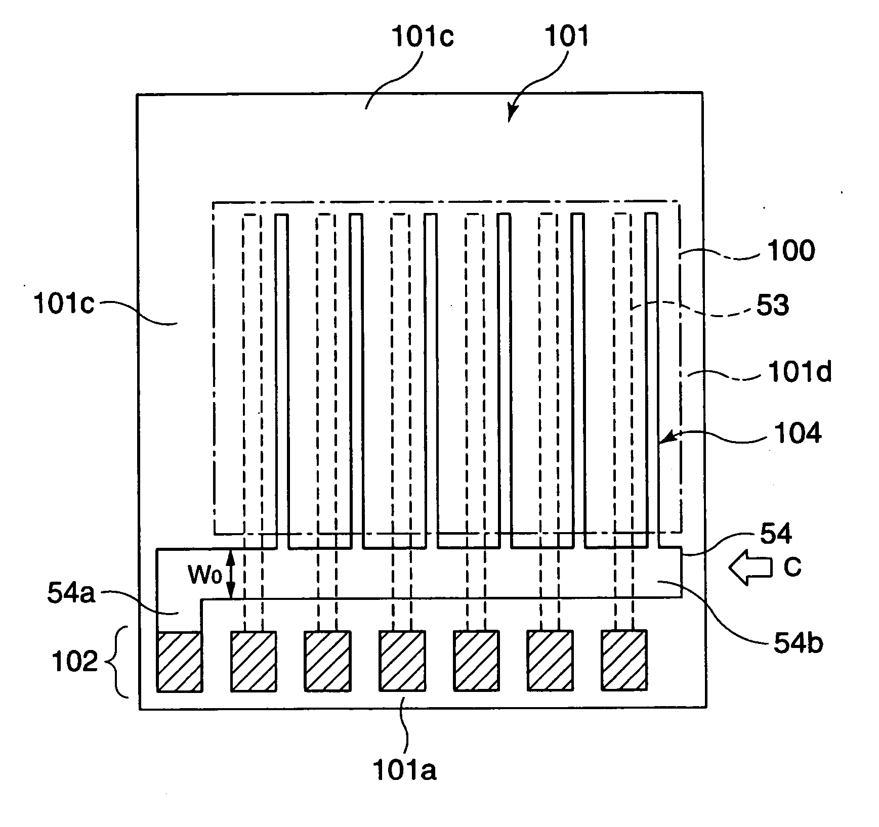
[0066] FIG. 1 illustrates an electro-optical device according to a first embodiment of the present invention. In FIG. 1, the same reference numerals indicate the same elements as those of FIG. 18.

[0067] The basic structure of the electro-optical device according to the present embodiment is almost the same as that of a conventional electro-optical device illustrated in FIG. 18. However, the electro-optical device according to the present embodiment includes a second power source bus line 54 connected to a mounting terminal portion 102 connected to the first region 101a instead of the first power source bus line 103 illustrated in FIG. 18.

[0068] As illustrated in FIG. 1, the second power source bus line 54 consists of one continuous conductive line and is made of a metal such as Al or AlSiCu. The second power source bus line 54 consists of a first conductive portion 54a with one end connected to the connecting portion of the mounting terminal portion 102 and ...

second embodiment

of Electro-Optical Device

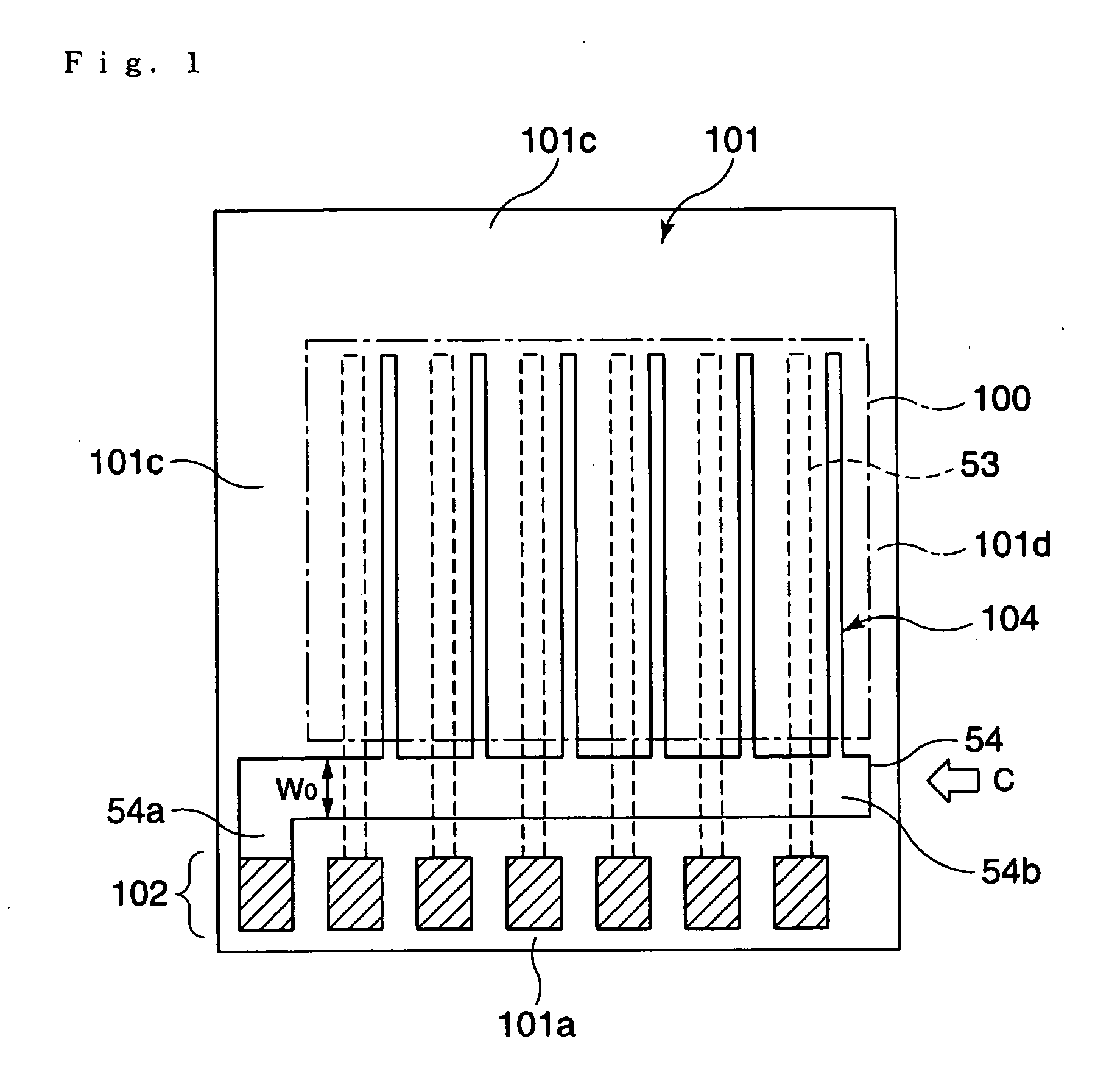
[0069] FIG. 2 illustrates an electro-optical device according to a second embodiment of the present invention. In FIG. 2, the same reference numerals indicate the same elements as those of FIG. 18.

[0070] The basic structure of the electro-optical device according to the present embodiment is almost the same as that of the conventional electro-optical device illustrated in FIG. 18. However, the electro-optical device according to the present embodiment includes a third power source bus line 10 connected to the second to fourth regions 101b, 101c, and 101d and connected to the mounting terminal portion 102 in two places instead of the first power source bus line 103 illustrated in FIG. 18.

[0071] As illustrated in FIG. 2, the third power source bus line 10 consists of one continuous conductive line and is made of a metal such as Al or AlSiCu. The third power source bus line 10 consists of a first conductive portion 10a whose both ends are connected to the conne...

third embodiment

of Electro-Optical Device

[0078] FIG. 4 illustrates an electro-optical device according to a third embodiment of the present invention. In FIG. 4, the same reference numerals indicate the same elements as those of FIG. 2.

[0079] The basic structure of the electro-optical device according to the present embodiment is almost the same as that of the electro-optical device according to the second embodiment illustrated in FIG. 2. The electro-optical device according to the present embodiment includes a fourth power source bus line 20 arranged in the first region 101a and connected to the mounting terminal portion 102 in two places instead of the third power source bus line 10 illustrated in FIG. 2.

[0080] As illustrated in FIG. 4, a fourth power source bus line 20 consists of one continuous conductive line and is made of a metal such as Al or AlSiCu. Further, the fourth power source bus line 20 has both ends connected to a connecting portion (not shown) of the mounting terminal portion 102...


PUM


Abstract

To provide an electro-optical device and an electronic apparatus capable of maintaining the display quality by preventing brightness unevenness without widening a frame. In a mounting terminal portion 102 connection portions (not shown) connecting to a fourth power source bus line 20 are provided in twoplaces. Driving current is supplied from the connection portions to the fourth power source bus line 20. The width of the fourth power source bus line is smaller than that of the width of a power source bus line supplying driving current from one place of the mounting terminal portion.

Description

[0001] The present invention relates to electro-optical devices and electronic apparatues, and more specifically, it relates to an electro-optical device for driving a current-driven element and to an electronic apparatus.DESCRIPTION OF THE PRIOR ART[0002] Conventionally, various electro-optical devices such as organic EL panels with current-driven elements have been disclosed. As illustrated in FIG. 18, a conventional electro-optical device includes a matrix display portion 100 with a plurality of current-drive elements (not shown), a frame portion 101 formed at the periphery of the matrix display portion 100, a mounting terminal portion 102 provided at one edge of the frame portion 101, a power source bus line 103 which is a conductive line arranged in the frame portion 101 and which is connected to the mounting terminal portion 102, and n (n.gtoreq.1) power source lines 104 connected to the power source bus line 103, the power source lines 104 supplying driving current to the cur...

Claims


Application Information

Patent Timeline
Patent Type & Authority Applications(United States)
IPC IPC(8): G09F9/30H01L51/50G09G3/20H01L27/32H05B44/00
CPCG09G3/20G09G2300/04H01L27/3279G09G2320/0233G09G2320/0223H10K59/1315G09G3/30
Inventor HIRAYAMA, HIROSHI
Owner SEIKO EPSON CORP
Why Eureka
Try Eureka