Analog delay locked loop having duty cycle correction circuit

a technology of duty cycle and locked loop, which is applied in the direction of digital storage, instruments, generating/distributing signals, etc., can solve the problems of low performance of synchronous semiconductor memory devices, delay of internal clock signals in comparison with external clock signals, etc., and achieve the effect of reducing the initial time for locking the dll and widening the duty error rang

Inactive Publication Date: 2004-08-12
SK HYNIX INC
View PDF20 Cites 27 Cited by
  • Summary
  • Abstract
  • Description
  • Claims
  • Application Information

AI Technical Summary

Benefits of technology

0017] It is, therefore, an object of the present invention to provide a delay locked loop (DLL)...

Problems solved by technology

However, the internal clock signal is delayed in comparison with the external clock signal because of passing through internal circuits included in the synchronous semiconductor memory device.
The delayed internal ...

Method used


Image

  • Analog delay locked loop having duty cycle correction circuit
  • Analog delay locked loop having duty cycle correction circuit
  • Analog delay locked loop having duty cycle correction circuit

Examples


Embodiment Construction

[0030] Hereinafter, an analog delay locked loop (DLL) device in accordance with the present invention will be described in detail referring to the accompanying drawings.

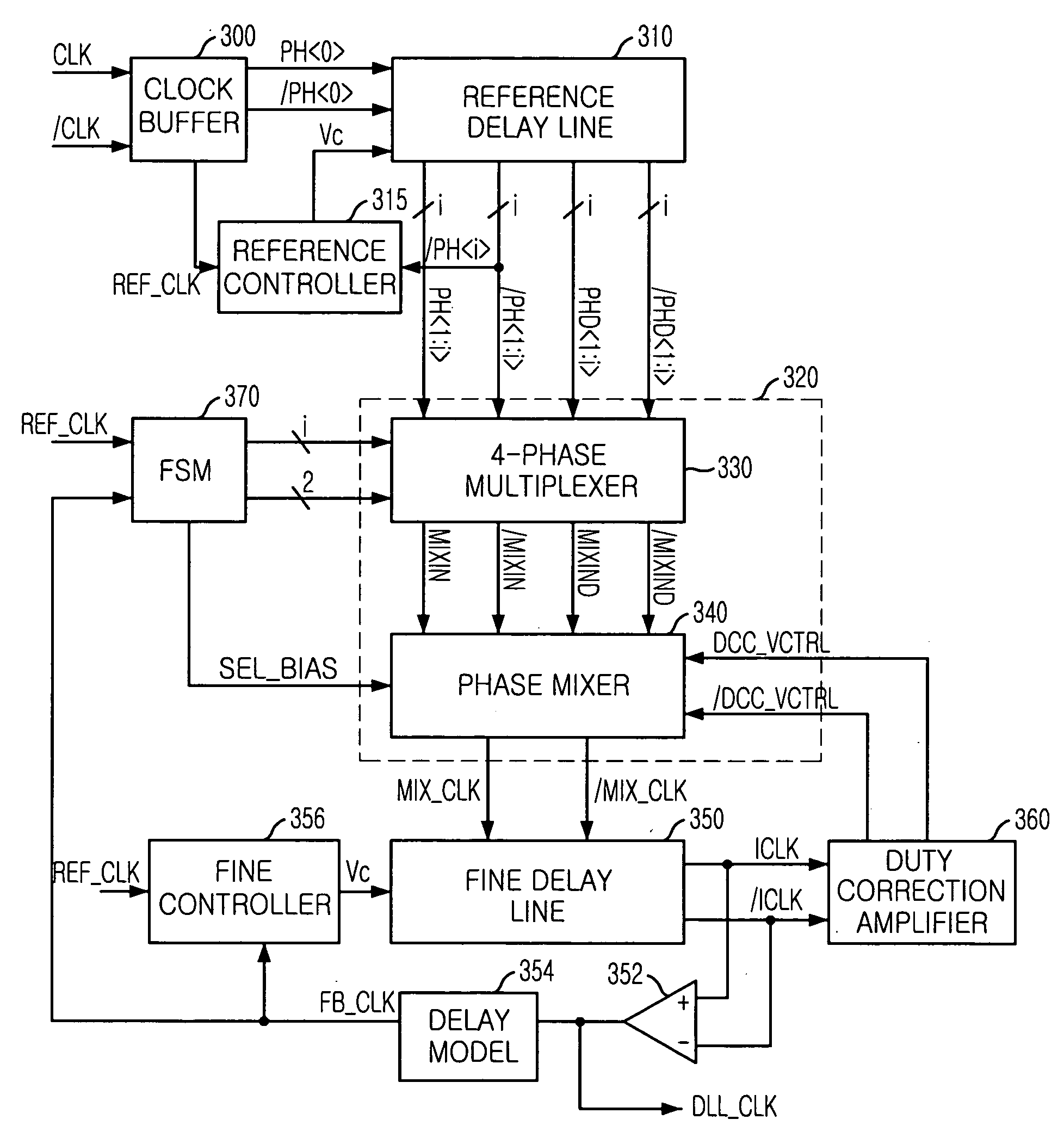
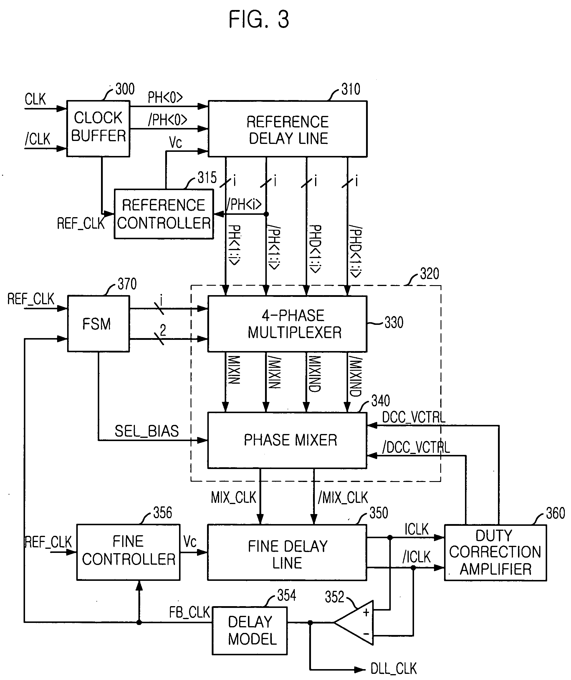
[0031] FIG. 3 is a block diagram showing an analog DLL device in accordance with an embodiment of the present invention.

[0032] As shown, the analog DLL device includes a clock buffer 300, a reference delay line 310, a reference controller 315, a clock interface 320, a fine delay line 350, a differential amplifier 352, a duty correction amplifier 360, a delay model 354, a fine controller 356 and a finite state machine FSM 370.

[0033] The clock buffer 300 receives an external clock signal pair CLK and / CLK in order to output an internal clock signal pair PH and / PH and a reference clock signal. REF_CLK. The reference clock signal REF_CLK and the internal clock signal PH are the same, i.e., thereby the reference clock signal REF_CLK can be substituted by the internal clock signal PH.

[0034] The reference delay line 310 re...


PUM


Abstract

An analog delay locked loop device includes a first block for receiving an internal clock signal and a reference clock signal to generate normal multi phase clock signal pairs and dummy multi phase clock signal pairs; and a second block for receiving the reference clock signal to generate a delay locked internal clock signal having a corrected duty cycle based on the normal multi phase clock signal pairs and the dummy multi phase clock signal pairs.

Description

[0001] The present invention relates to a semiconductor device; and, more particularly, to an analog delay locked loop (DLL) device having a duty cycle correction (DCC) circuit.DESCRIPTION OF PRIOR ART[0002] A synchronous semiconductor memory device which is operated synchronizing with an external clock signal receives the external clock signal and uses an internal clock signal generated from the received external clock signal. However, the internal clock signal is delayed in comparison with the external clock signal because of passing through internal circuits included in the synchronous semiconductor memory device. The delayed internal clock signal causes low performance of the synchronous semiconductor memory device.[0003] Therefore, the synchronous semiconductor memory device should be provided with an apparatus for synchronizing the internal clock signal with the external clock signal.[0004] Generally, a delay locked loop (DLL) device or a phase locked loop (PLL) device is prov...

Claims


Application Information

Patent Timeline
IPC IPC(8): G06F1/04G11C11/407H03K5/05H03K5/135H03K5/156H03L7/00H03L7/06H03L7/07H03L7/08H03L7/081
CPCH03K5/1565H03L7/0814H03L7/0812H03L7/07H03L7/0816H03L7/08
Inventor KIM, SE-JUNHONG, SANG-HOONKO, JAE-BUM
Owner SK HYNIX INC
Why Eureka
Try Eureka