Gas recovery system to improve the efficiency of abatementand/or implement reuse/reclamation

a gas recovery system and abatement efficiency technology, applied in the field of gas recovery system, can solve the problems of low utilization rate of feed materials, adversely affecting the process system, low utilization rate, etc., and achieve the effect of improving the abatement efficiency

Inactive Publication Date: 2004-09-30
APPLIED MATERIALS INC
View PDF22 Cites 9 Cited by
  • Summary
  • Abstract
  • Description
  • Claims
  • Application Information

AI Technical Summary

Benefits of technology

0014] A further aspect of the invention relates to a gas recovery system for improving the efficiency of abatement and / or implementing reclamation and reuse of unused feed material in effluent of a semiconductor manufacturing facility, such system comprising an unused feed material reclamation unit arranged to recover the unused feed material.
0015] Another aspect of the invention relates to a process for improving the efficiency of abatement and / or implementing reclamation and reuse of unused feed material in effluent of a semiconductor manufacturing facility, such process comprising recovering the unused feed material from the effluent.

Problems solved by technology

This low rate of utilization of feed materials adversely affects the process system in many ways.
For example, low utilization. rates represent increased costs of operation of the semiconductor manufacturing plant, relative to a plant in which higher levels of utilization are achieved.
Further, low utilization rates mean that unused raw materials in the effluent present a large burden on effluent treatment systems, e.g., by increasing the volume of the exhaust stream that must be treated, and the type and variety of effluent waste species, thereby multiplying the corresponding treatment requirements relative to a process in which the raw materials are at low or negligible levels in the effluent.
In addition, the capital costs of the semiconductor manufacturing process facility are increased, since vessels, lines, pumps, reservoirs, etc. must be sized for the overall flow of process feed materials, and thus must be larger than in the case where higher overall utilization of the feed materials is achieved.
Correspondingly, the energy costs of the process facility are increased, to effect heating, cooling, neutralization, volatilization, etc., of larger flows of materials in the process facility, due to the presence of non-utilized feed materials in the streams flowing through the process facility.
Even when the effluent concentrations of unused feed materials are small, the presence of such materials nonetheless represents a waste of the feed materials that adversely impacts the semiconductor manufacturing operation and in many instances imposes a burden on the environment.
To remove specific impurities to non-harmful levels in conventional practice often requires a process-intensive solution, with respect to energy, water, equipment size, etc.
It is apparent that wastage of feed materials in the effluent from the process is a severe deficiency that adversely impacts the economics of conventional semiconductor manufacturing facilities.

Method used


Image

  • Gas recovery system to improve the efficiency of abatementand/or implement reuse/reclamation
  • Gas recovery system to improve the efficiency of abatementand/or implement reuse/reclamation
  • Gas recovery system to improve the efficiency of abatementand/or implement reuse/reclamation

Examples


Embodiment Construction

, and Preferred Embodiments Thereof

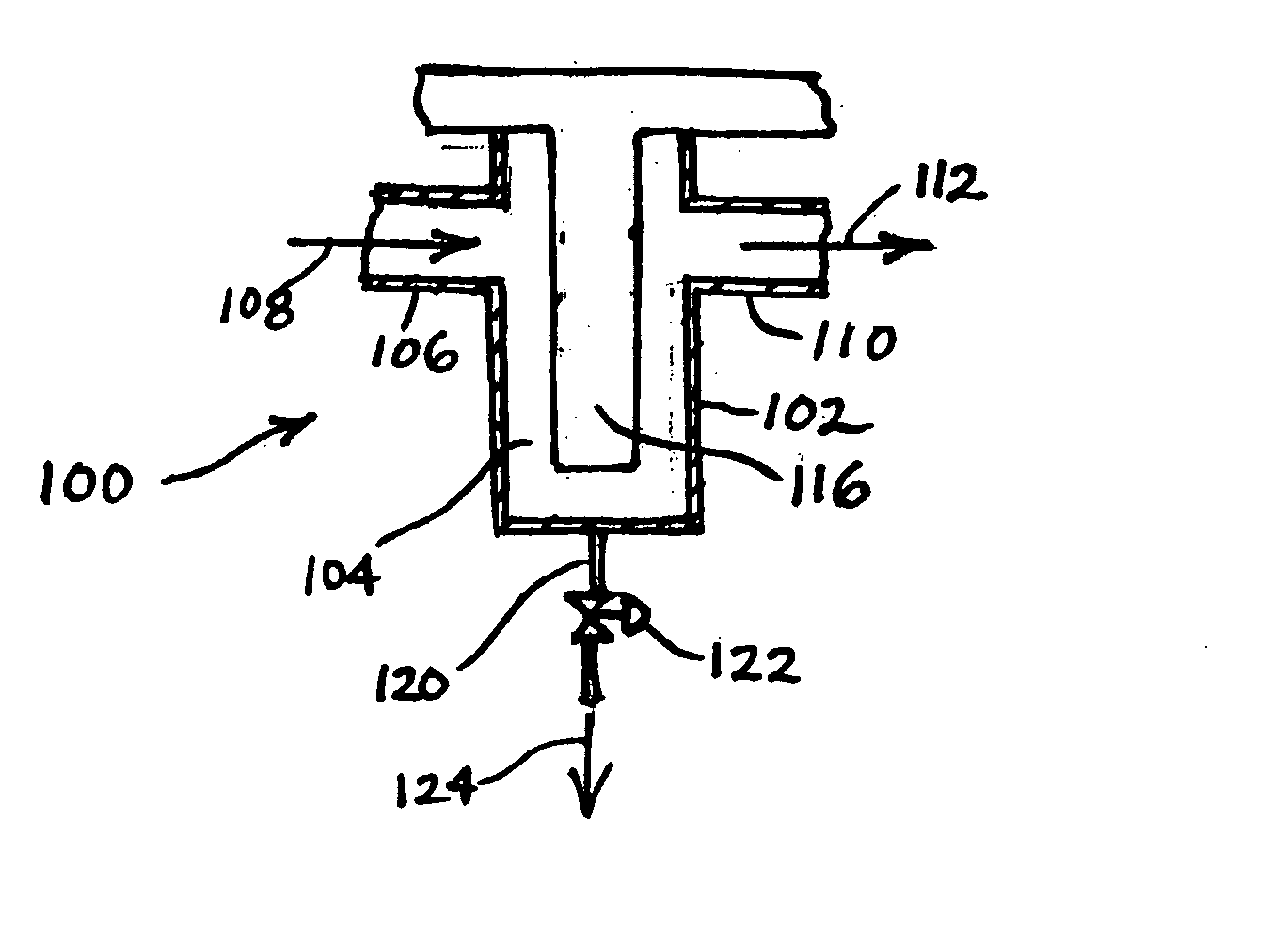
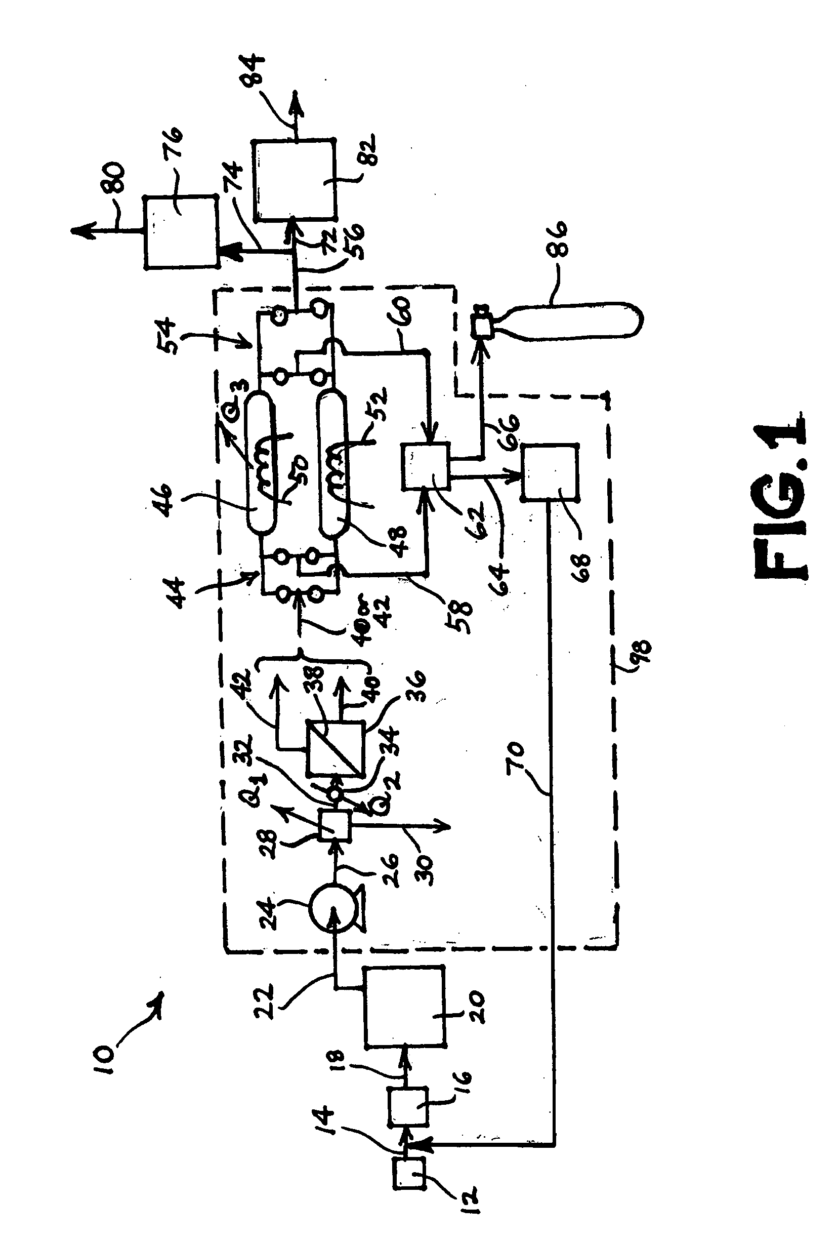
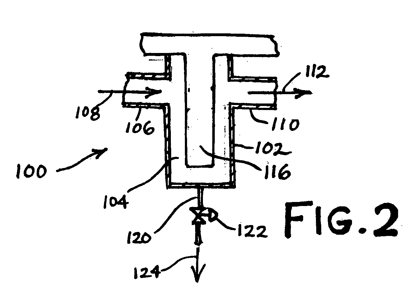
[0022] The method and apparatus of the present invention are usefully employed for recovery and utilization of unused feed materials in the effluent of a semiconductor manufacturing facility, thereby reclaiming feed materials furnished to the facility that escape active processing and, in the absence of the recovery and utilization approach of the present invention, would simply pass through the facility and be discharged to the facility's waste treatment system(s), e.g., a point-of-use abatement unit of a semiconductor manufacturing tool in such facility.

[0023] The method and apparatus of the invention correspondingly achieve a substantial reduction in the cost of manufacturing semiconductor products, by achieving reductions in the requirements of effluent abatement and disposal for the semiconductor manufacturing facility. Further, since the recovered feed materials have significant value when reclaimed and reused, the present invention also achi...


PUM


Abstract

A gas recovery system for improving the efficiency of abatement and/or implementing reclamation and reuse of unused feed materials in effluent of a semiconductor manufacturing facility, especially in instances in which substantial portions of feed material are unused. The effluent is treated to reversibly capture the unused feed material, e.g., at a capture locus such as a physical adsorbent, cold finger, cryotrap, heat exchanger/condenser, membrane separation unit, filter, etc., and the captured unused feed material then is released from the capture locus and processed for such abatement and/or reclamation and reuse.

Description

BACKGROUND OF INVENTION[0001] The present invention relates to method and apparatus for recovering constituents of effluent streams from semiconductor manufacturing operations, to improve the efficiency of abatement of the effluent and / or to implement reuse and / or reclamation of effluent components, e.g., by recovery of unreacted / unconsumed feed components that would otherwise pass unused through the semiconductor manufacturing process into the effluent that is abated or discharged from the semiconductor manufacturing process facility.DESCRIPTION OF THE RELATED ART[0002] Most chemical vapor deposition (CVD) and metalorganic chemical vapor deposition (MOCVD) processes use only a small portion of the feed gases / chemicals supplied to such processes, e.g. 50% or less. This low rate of utilization of feed materials adversely affects the process system in many ways.[0003] For example, low utilization. rates represent increased costs of operation of the semiconductor manufacturing plant, r...

Claims


Application Information

Patent Timeline
Patent Type & Authority Applications(United States)
IPC IPC(8): B01D53/02
CPCB01D53/02
Inventor WANG, LUPINGARNO, JOSE I.OLANDER, W. KARLTOM, GLENN M.
Owner APPLIED MATERIALS INC
Why Eureka
Try Eureka