Thin-film magnetic head and method of manufacturing same, and thin-film magnetic head substructure
a technology of thin film and magnetic head, which is applied in the direction of heads with metal sheet cores, instruments, nanoinformatics, etc., can solve the problems of increasing the resistance of the coil, affecting the writing effect, and the inability to effectively use the flux generated by the coil for writing, etc., to achieve excellent writing characteristics, reduce the length of the magnetic path, and reduce the effect of resistan
- Summary
- Abstract
- Description
- Claims
- Application Information
AI Technical Summary
Benefits of technology
Problems solved by technology
Method used
Image

Examples
second embodiment
[0203] Reference is now made to FIG. 29A to FIG. 37A and FIG. 29B to FIG. 37B to describe the invention. FIG. 29A to FIG. 37A are cross sections taken along a line the same as that of each of FIG. 2A to FIG. 17A. FIG. 29B to FIG. 37B are cross sections of magnetic pole portions each of which is parallel to the air bearing surface.
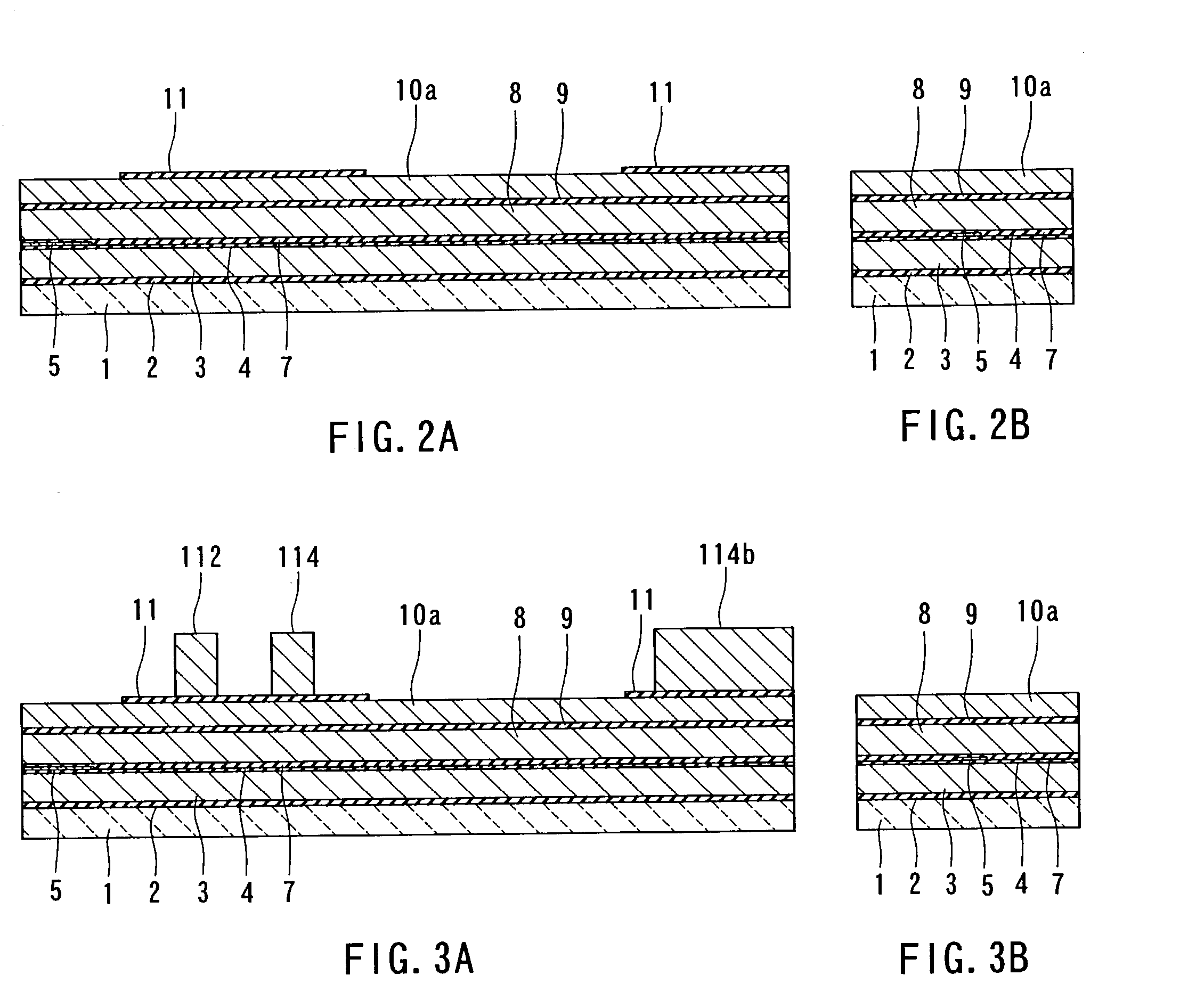
[0204] As shown in FIG. 5A and FIG. 5B, a method of manufacturing a thin-film magnetic head of the second embodiment includes the steps the same as those of the first embodiment that are performed until the first layer 10a is selectively etched through the use of the photoresist layer 12 as a mask to pattern the first layer 10a.
[0205] In the second embodiment, the photoresist layer 12 is removed, and an insulating film 61 made of alumina, for example, is then formed by CVD, for example, so as to cover the entire top surface of the layered structure as shown in FIG. 29A and FIG. 29B. As a result, grooves covered with the insulating film 15 are formed in the ...
first embodiment
[0211] Next, frame plating, for example, is performed to form the fourth layer 10d on the second layer 10b, form the fifth layer 10e on the third layer 10c, and form the first connecting portion layers on the respective contact portions of the conductor portions 111 to 115. FIG. 32A shows the connecting portion layer 18a that is one of the first connecting portion layers formed on the contact portion 114b of the conductor portion 114. The fourth layer 10d, the fifth layer 10e and the first connecting portion layers may be made of a material the same as that of the
[0212] Next, the insulating layer 20 made of alumina, for example, and having a thickness of 2 to 3 .mu.m, for example, is formed to cover the entire top surface of the layered structure. The insulating layer 20 is then polished by CMP, for example, so that the fourth layer 10d, the fifth layer 10e, and the first connecting portion layers are exposed.
[0213] Next, as shown in FIG. 33A and FIG. 33B, the magnetic layer 21 made...
third embodiment
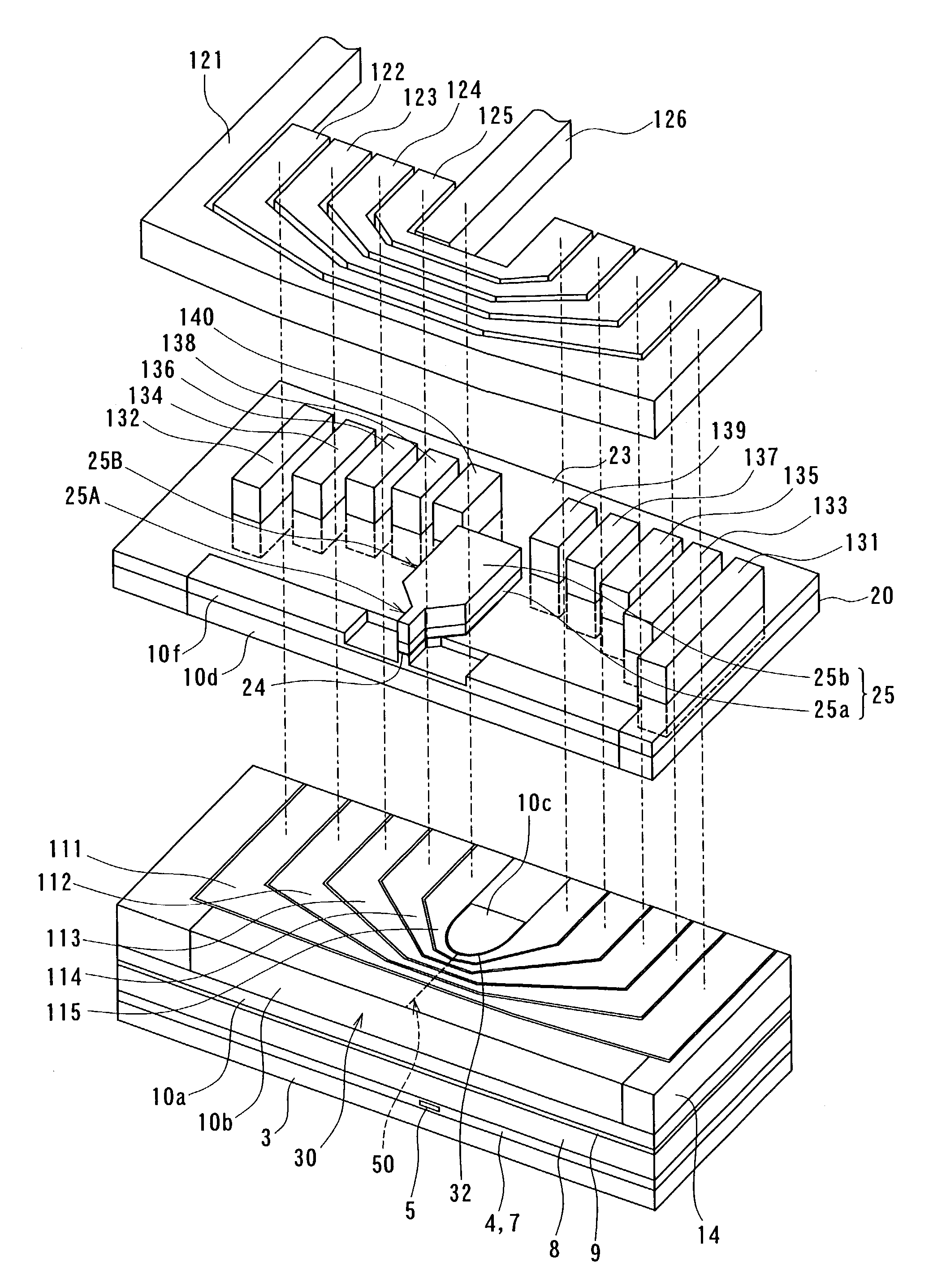
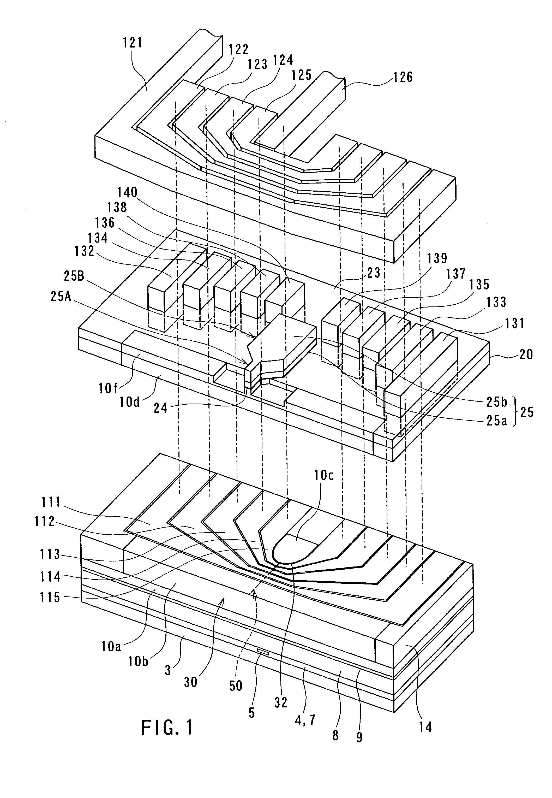
[0230] Reference is now made to FIG. 38 and FIG. 39 to describe a third embodiment of the invention. FIG. 38 is a plan view showing the inner conductor portions and the connecting portions of the thin-film coil of the third embodiment. FIG. 39 is a plan view showing the outer conductor portions of the thin-film coil of the embodiment.
[0231] The thin-film magnetic head of the embodiment comprises the three-turn thin-film coil in place of the five-turn coil 110 of the first embodiment. The coil of the third embodiment has the inner conductor portions 111 to 113, the outer conductor portions 121 to 123, and the connecting portions 131 to 136.
[0232] The inner conductor portions 111 to 113 are disposed side by side and extend in the direction intersecting the direction orthogonal to the air bearing surface (that is, the horizontal direction of FIG. 38). The inner conductor portions 111 to 113 have contact portions 111a to 113a provided near ends of the respective inner conductor portions...
PUM
| Property | Measurement | Unit |
|---|---|---|
| thickness | aaaaa | aaaaa |
| thickness | aaaaa | aaaaa |
| thickness | aaaaa | aaaaa |
Abstract
Description
Claims
Application Information
 - R&D
- Intellectual Property
- Life Sciences
- Materials
- Tech Scout
- Unparalleled Data Quality
- Higher Quality Content
- 60% Fewer Hallucinations
Browse by: Latest US Patents, China's latest patents, Technical Efficacy Thesaurus, Application Domain, Technology Topic, Popular Technical Reports.
© 2025 PatSnap. All rights reserved.Legal|Privacy policy|Modern Slavery Act Transparency Statement|Sitemap|About US| Contact US: help@patsnap.com