

Method of fabricating semiconductor side wall fin
a metal oxide semiconductor and side wall fin technology, applied in the direction of transistors, semiconductor devices, electrical equipment, etc., can solve the problems of poor quality, poor control device, poorer quality, etc., and achieve the effect of tight tolerances on channel thickness and no complicated epitaxial growth
- Summary
- Abstract
- Description
- Claims
- Application Information
AI Technical Summary
Benefits of technology
Problems solved by technology
Method used
Image

Examples
Embodiment Construction
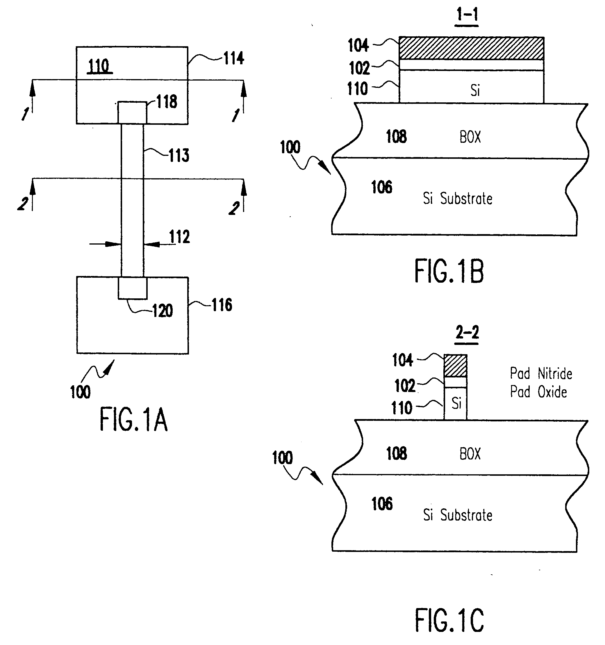
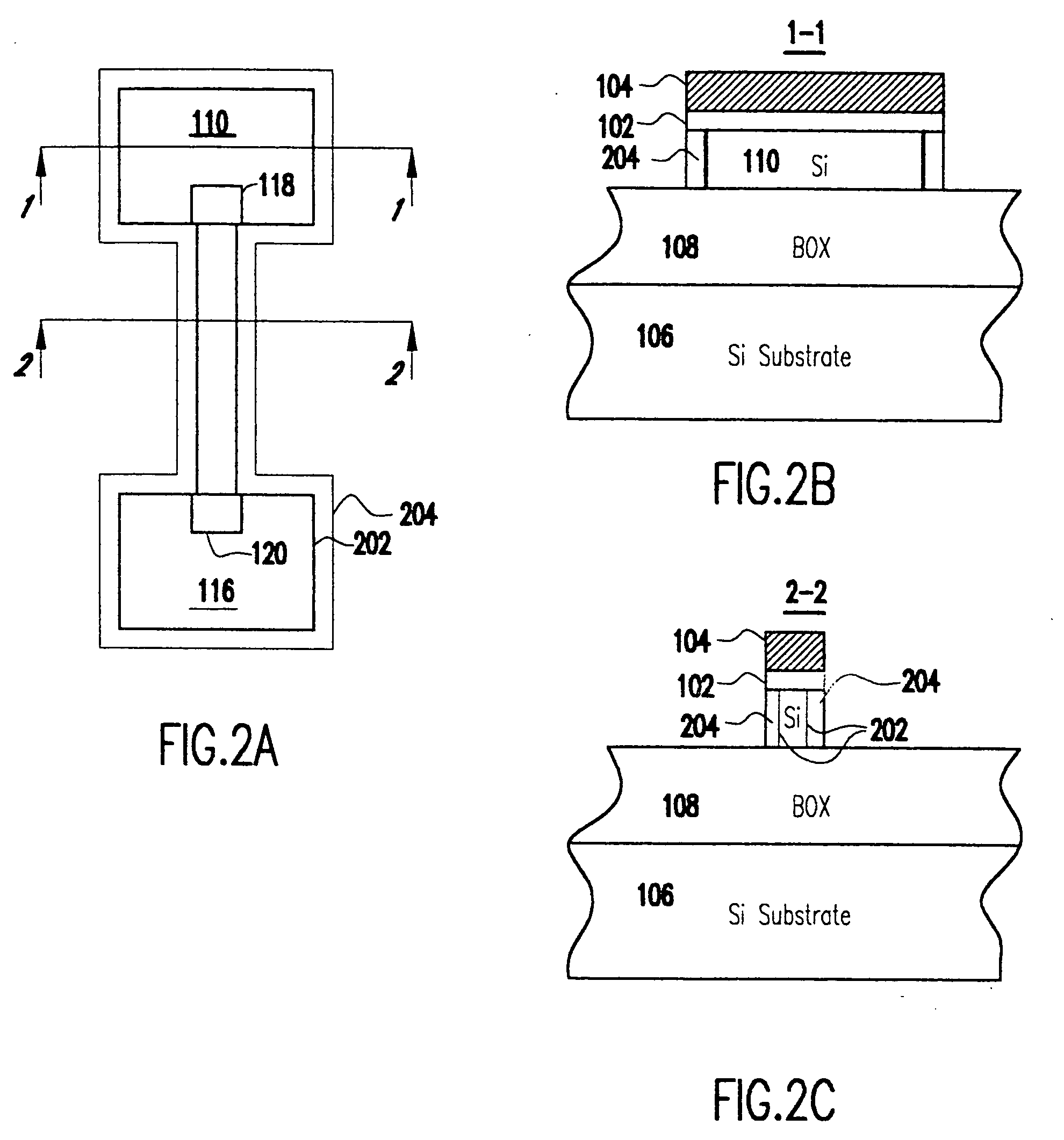
[0046] Referring now to FIG. 1A, there is shown a top view of a starting silicon-on-insulator (SOI) substrate 100. As shown in FIGS. 1B and 1C, which correspond to sections 1-1 and 2-2 shown in FIG. 1A, respectively, the substrate 100 is comprised of a bulk substrate 106, a buried oxide (BOX) 108 layer, and an active layer 110. FIGS. 1B and 1C also show an oxide pad film 102 and a nitride pad film 104 on active layer 110. Those skilled in the art will realize that it may be preferable to have the oxide pad film 102 placed on top of the nitride pad film 104. The pad oxide 102 is grown using standard oxidation techniques and would typically be in the range of 3 to 14 nm, with 8 nm being preferred. Pad films 104 are placed upon pad oxide 102. It is preferred that nitride films be utilized as pad films 104, although other materials may also be used. The nitride (upper) pad films 104 are typically in the range of 30 to 120 nm, with 80 nm being preferred, and define the etch areas for sha...
PUM
 Abstract
Description
Claims
Application Information