Liquid crystal display and electronic device

Active Publication Date: 2005-01-27
BOE TECH GRP CO LTD
View PDF10 Cites 7 Cited by
  • Summary
  • Abstract
  • Description
  • Claims
  • Application Information

AI Technical Summary

Benefits of technology

[0014] The liquid crystal display of the present invention is a combination of a transflective liquid crystal display and a liquid crystal in a vertical alignment mode. A transflective liquid crystal display can be provided with a structure in which, in order to address or solve the problem of reduction in contrast due to the difference of retardation between the reflective and the transparent display modes, the thickness of the liquid crystal layer is varied in the reflective display area and in the transparent display area by forming an insulating film with a fixed thickness in the reflective display area on the lower substrate so as to project toward the liquid crystal layer. The applicants have studied this type of liquid crystal display. With such a structure, the thickness of the liquid crystal layer in the reflective display area can be made to be smaller than that of the liquid crystal layer in the transparent display area owing to the presence of the insulating film. Therefore, the retardation in the reflective display area and the retardation in the transparent display area can be sufficiently close to or substantially equal to each other, thereby allowing an increase in contrast.
[0034] Furthermore, providing a circularly-polarized-light radiating device to radiate circularly polarized light to the one substrate or the other substrate allows preferable reflective display and transparent display.

Problems solved by technology

However, problems exist with such a structure, including a problem of decreased contrast due to the difference in retardation in the reflective and transparent display modes, problems of alignment control and alignment division in the vertical alignment mode, and so on, thus preventing such a display from becoming realized.

Method used


Image

  • Liquid crystal display and electronic device
  • Liquid crystal display and electronic device
  • Liquid crystal display and electronic device

Examples


Embodiment Construction

[0053] Referring to FIGS. 1 to 3, a first exemplary embodiment of the present invention is described below.

[0054] A liquid crystal display of this exemplary embodiment is an example of an active-matrix liquid crystal display that uses a thin film transistor (hereinafter “TFT”) as a switching element.

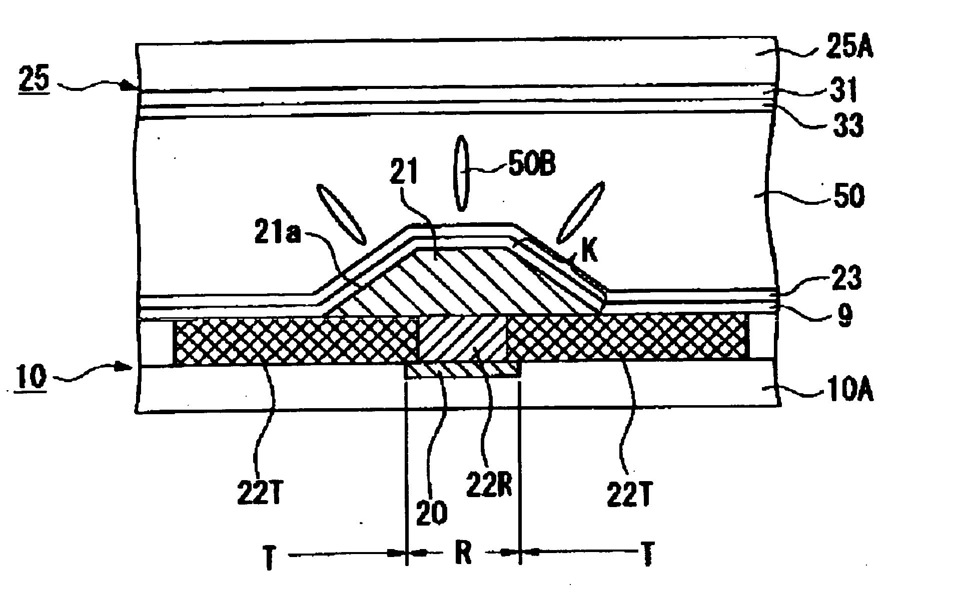
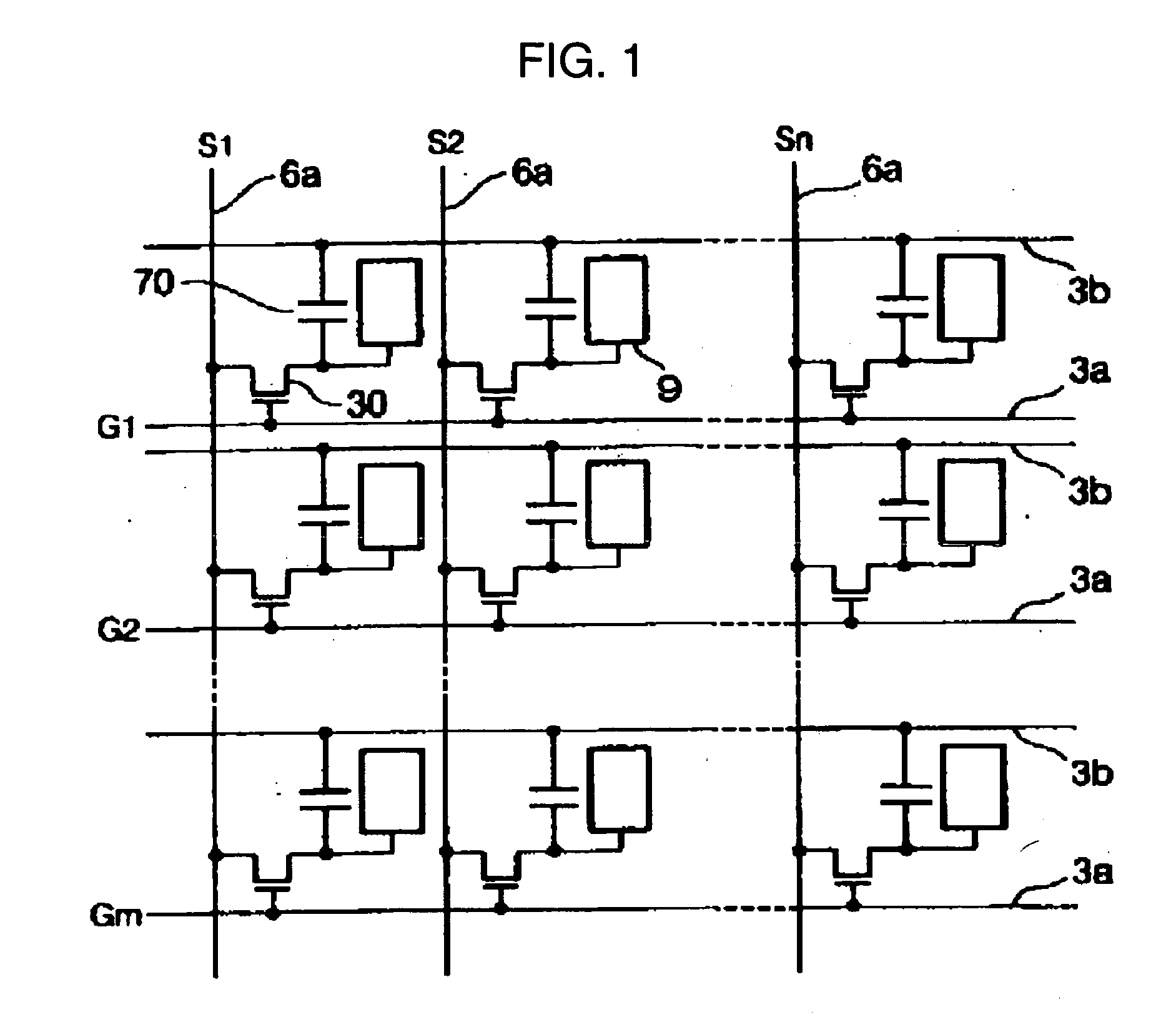
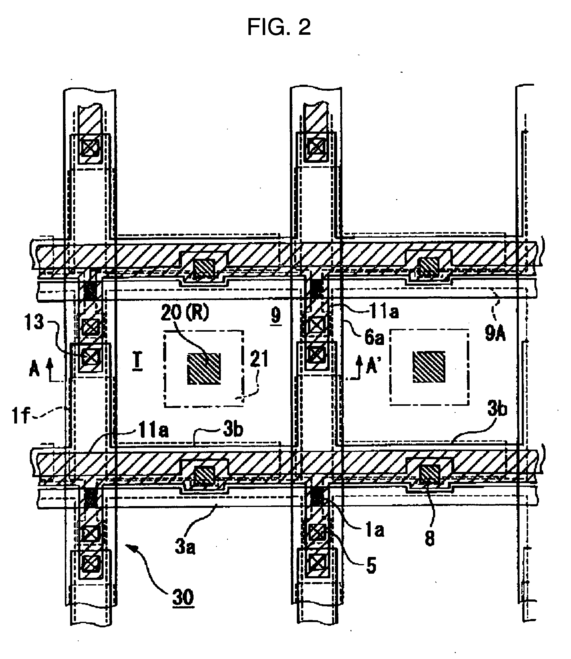
[0055]FIG. 1 is a schematic circuit diagram of a plurality of dots arranged in the form of matrix which constitute an image display area of the liquid crystal display according to this exemplary embodiment. FIG. 2 is a plan view showing the structure of the adjacent plurality of dots on a TFT array substrate. FIG. 3 is a sectional view taken along plane A-A′ of FIG. 2, showing the structure of the liquid crystal display. In the following drawings, the layers and members are scaled variously in order to make them discernible on the drawings, and are not representative of their actual sizes.

[0056] In the liquid crystal display of this exemplary embodiment, each of the plurality of dots ...


PUM


Abstract

The invention provides a liquid crystal display capable of obtaining light and high-contrast display having a wide viewing angle in a transflective liquid crystal display. A liquid crystal display of the present invention employs a vertical alignment mode using a liquid crystal layer that is vertically aligned in the initial alignment state. A transparent display area is disposed to surround the periphery of a reflective display area in one dot, and an insulating film is provided in the area that corresponds to the reflective display area in the center of the dot. The insulating film makes the thickness of the liquid crystal layer in the reflective display area to be smaller than the thickness of the liquid crystal layer in the transparent display area.

Description

[0001] This is a Division of application Ser. No. 10 / 352,199 filed Jan. 28, 2003. The entire disclosure of the prior application is hereby incorporated by reference herein in its entirety.BACKGROUND OF THE INVENTION [0002] 1. Field of Invention [0003] The present invention relates to a liquid crystal display and an electronic device. More specifically, the invention relates to a technique of obtaining a high-contrast display having a wide viewing angle in a transflective liquid crystal display that performs display in both a reflective mode and a transparent mode. [0004] 2. Description of Related Art [0005] Since reflective liquid crystal displays have no light sources, such as a backlight, they consume low power, and thus can be used for various portable electronic devices. However, the reflective liquid crystal displays perform display using outside light, such as sunlight and illumination light. Thus, these displays are subject to low visibility in a dark place. Therefore, the re...

Claims


Application Information

Patent Timeline
IPC IPC(8): G02F1/1335G02F1/139G02F1/1333
CPCG02F1/133345G02F1/133371G02F2203/09G02F1/1393G02F2001/133776G02F1/133555G02F1/133776G02F1/1335
Inventor OZAWA, KINYAURANO, NOBUTAKAMAEDA, TSUYOSHI
Owner BOE TECH GRP CO LTD
Why Eureka
Try Eureka