Semiconductor device including reference voltage generation circuit attaining reduced current consumption during stand-by
- Summary
- Abstract
- Description
- Claims
- Application Information
AI Technical Summary
Benefits of technology
Problems solved by technology
Method used
Image

Examples
Example
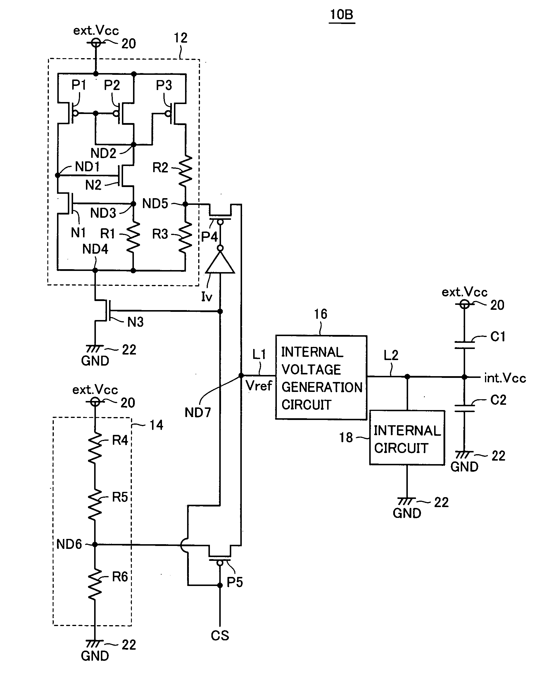
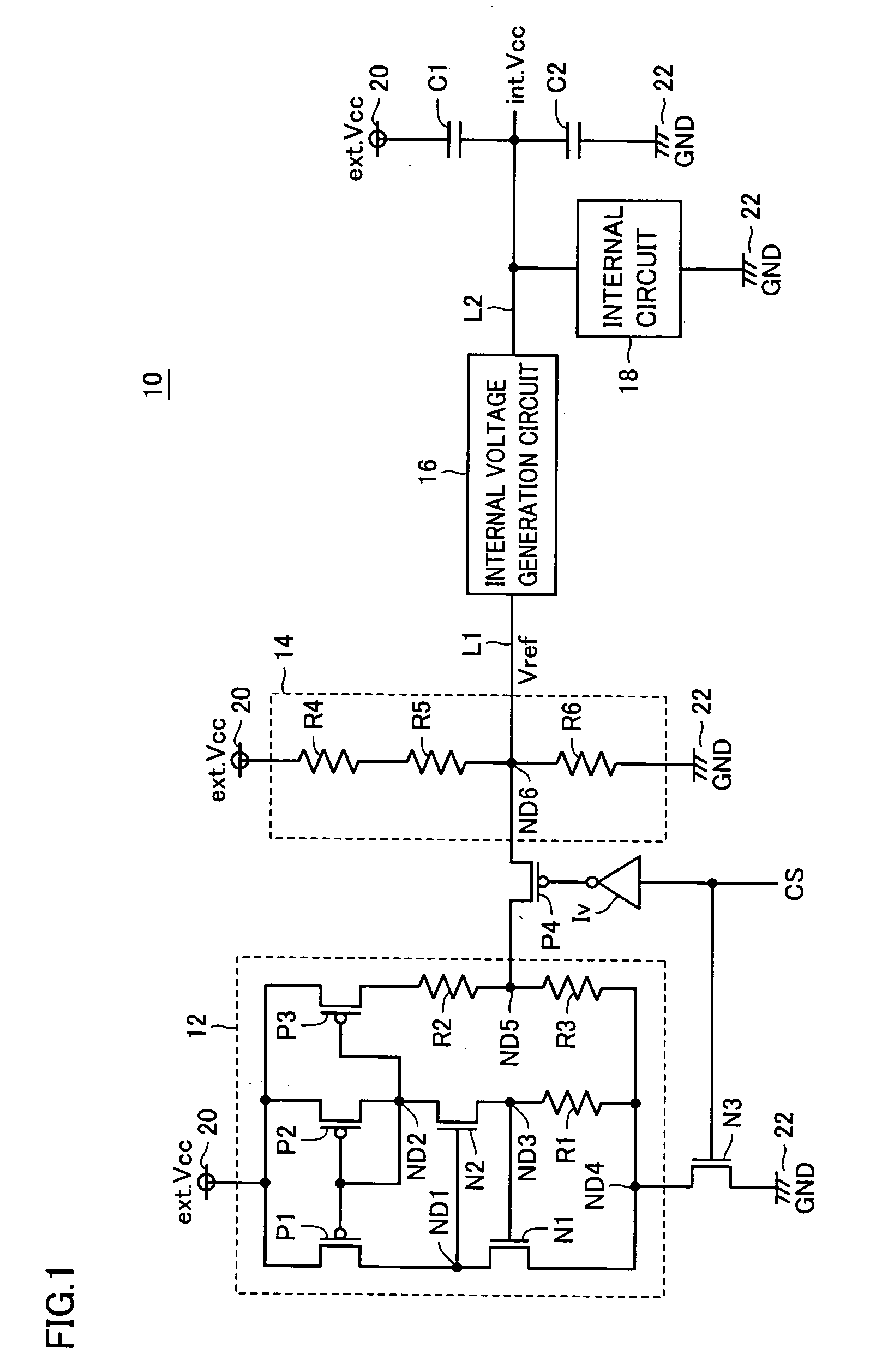
[0023]FIG. 1 is a circuit diagram showing a configuration of a main portion of a semiconductor device 10 in a first embodiment of the present invention.
[0024] Referring to FIG. 1, semiconductor device 10 includes a first reference voltage generation circuit 12, a second reference voltage generation circuit 14, an N-channel MOS transistor N3, a P-channel MOS transistor P4, an inverter Iv, an internal voltage generation circuit 16, an internal circuit 18, a reference voltage line L1, an internal power supply line L2, and capacitors C1, C2.
[0025] First reference voltage generation circuit 12 includes P-channel MOS transistors P1 to P3, N-channel MOS transistors N1, N2, and resistors R1 to R3. Second reference voltage generation circuit 14 includes resistors R4 to R6.
[0026] First reference voltage generation circuit 12 is a voltage generation circuit of threshold voltage reference type. P-channel MOS transistor P1 is connected between a power supply node 20 to which an external power...
Example
[0052] Second Embodiment
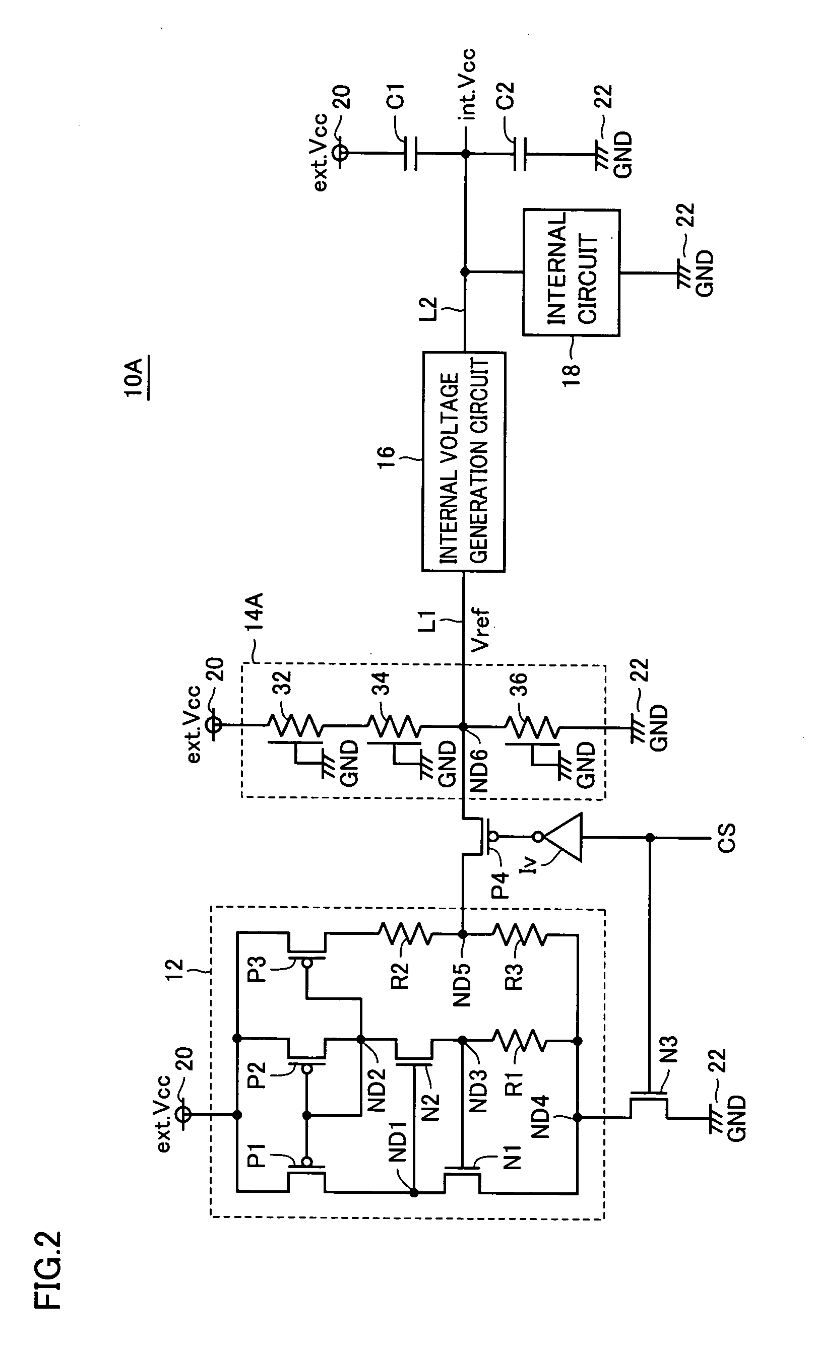
[0053]FIG. 2 is a circuit diagram showing a configuration of a main portion of a semiconductor device 10A in a second embodiment of the present invention.
[0054] Referring to FIG. 2, semiconductor device 10A includes a second reference voltage generation circuit 14A instead of second reference voltage generation circuit 14 in the configuration of semiconductor device 10 in the first embodiment. The configuration of semiconductor device 10A is otherwise the same as that of semiconductor device 10.
[0055] Second reference voltage generation circuit 14A includes P-channel thin film transistors (hereinafter, the thin film transistor is also referred to as “TFT (Thin Film Transistor)”) 32 to 36. P-channel TFT 32 is connected between power supply node 20 and P-channel TFT 34, and receives ground voltage GND at its gate. P-channel TFT 34 is connected between P-channel TFT 32 and node ND6, and receives ground voltage GND at its gate. P-channel TFT 36 is connected be...
Example
[0068] Third Embodiment
[0069] An overall configuration of a semiconductor device in a third embodiment is the same as that of semiconductor device 10A in the second embodiment shown in FIG. 2. Though the third embodiment also includes a memory unit storing data in internal circuit 18 as in the second embodiment, the memory unit in the third embodiment has a memory cell with a data holding characteristic during stand-by superior to that of the memory cell in the SRAM.
[0070]FIG. 4 is a circuit diagram showing a configuration of the memory cell in the memory unit contained in internal circuit 18 of the semiconductor device in the third embodiment.
[0071] Referring to FIG. 4, a memory cell 100 includes two adjacent data holding portions 102A, 102B storing one-bit data and inverted data thereof respectively. Data holding portion 102A is constituted of an N-channel MOS transistor 104A, a capacitor 106A, a charge compensation circuit 108A, and a storage node 110. Data holding portion 102...
PUM
 Abstract
Description
Claims
Application Information
 - R&D Engineer
- R&D Manager
- IP Professional
- Industry Leading Data Capabilities
- Powerful AI technology
- Patent DNA Extraction
Browse by: Latest US Patents, China's latest patents, Technical Efficacy Thesaurus, Application Domain, Technology Topic.
© 2024 PatSnap. All rights reserved.Legal|Privacy policy|Modern Slavery Act Transparency Statement|Sitemap