Differential signal squelch detection circuit and method
a detection circuit and signal technology, applied in the direction of digital transmission, line-fault/interference reduction, baseband system details, etc., can solve the problem that the output of the loss is often too slow to reliably detect the squelch sta
- Summary
- Abstract
- Description
- Claims
- Application Information
AI Technical Summary
Benefits of technology
Problems solved by technology
Method used
Image
Examples
Embodiment Construction
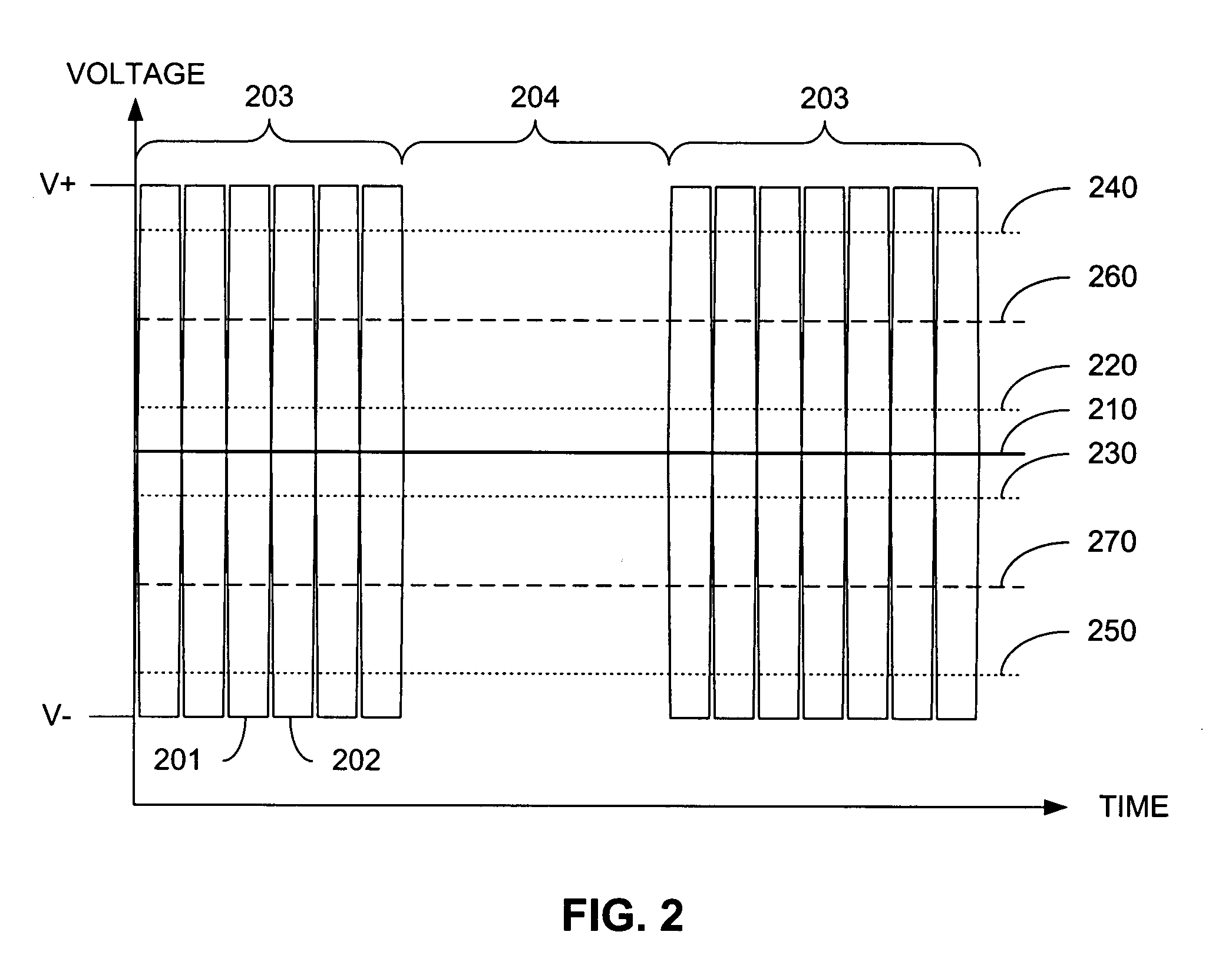
[0016] Before describing specific embodiments of the invention, a short discussion of the actions of the differential signal lines, “p” and “n”, during both the data transfer state and squelch, or out-of-band, state is desirable. As stated earlier, squelch state essentially is the state in which the “p” and “n” signal lines are not being driven to their normal data transmission voltage levels.
[0017]FIG. 2 graphically displays in an idealized fashion the action of the differential signal lines when in the data transfer state 203 and while in the squelch state 204. In typical differential signal fashion, the “p” signal waveform 201 and the “n” signal waveform 202, during the data transfer state 203, are essentially mirror images of each other across a midpoint voltage 210, existing substantially halfway between voltage levels V+ and V−. In other words, while the voltage of “p” signal waveform 201 is at V+, the voltage of the “n” signal waveform 202 is at V−, and vice-versa. To ensure...
PUM
 Abstract
Description
Claims
Application Information


