Method and apparatus for modeling devices having different geometries

a technology of geometries and devices, applied in adaptive control, process and machine control, instruments, etc., can solve the problems of overly complicated, burdensome traditional breadboard methods, and reduced individual device sizes,

Inactive Publication Date: 2005-02-03
CADENCE DESIGN SYST INC
View PDF13 Cites 35 Cited by
  • Summary
  • Abstract
  • Description
  • Claims
  • Application Information

AI Technical Summary

Benefits of technology

The present invention includes a new method for modeling devices having different geometries. In one embodiment of the present invention, the geometries of the devices to be modeled are in a geometrical space representing a range of channel lengths and channel widths, and the geometrical space is divided into a plurality of subregions each corresponding to a subrange of device geometrical variations. The plurality of subregions include a first set of subregions and a second set of subregions. The first or second set of subregions include one or more subregions. A regional global model is generated for each of the first set of subregions based on model equations and measurement data taken from a plurality of test devices. A binning model is generated for each of the second set of subregions based on model parameters extracted for one or more subregions in the first set of subregions. The regional global model for a subregion uses one set of model parameters to comprehend the subrange of device geometrical variations corresponding to the subregion. The binning model for a subregion includes binning parameters to provide continuity of the model parameters when device geometry varies across two different subregions.
The present invention also includes a computer readable medium comprising computer executable program instructions that when executed cause a digital processing system to perform a method for extracting semiconductor device model parameters. The method includes the steps of dividing a geometrical space including the different geometries into a first set of subregions and a second set of subregions, the first or the second set of subregions including one or more subregions; extracting a set of model parameters for each of the first set of subregions using model equations associated with the device model and measurement data obtained from a plurality of test devices; and determining binning parameters for each of the second set of subregions using one or more model parameters associated with one or more subregions in the first set of subregions.

Problems solved by technology

While the sizes of individual devices have decreased, the complexities of integrated circuits have increased at a dramatic rate over the past few decades.
As circuits have become more complex, traditional breadboard methods have become burdensome and overly complicated.
Although the binning model cards, when properly created, can accurately model device behavior in a broad range of device sizes, it is less scalable and involves many additional parameters that have no physical meanings.
Most importantly, since each binning model is created for its own bin in isolation from the creation of the binning models for the other bins, binning can result in discontinuity in device characteristics as the device geometry is varied across the boundaries of adjacent bins.
This discontinuity can complicate statistical analysis of device and circuit behavior and cause convergence problem during circuit simulation.

Method used


Image

  • Method and apparatus for modeling devices having different geometries
  • Method and apparatus for modeling devices having different geometries
  • Method and apparatus for modeling devices having different geometries

Examples


Embodiment Construction

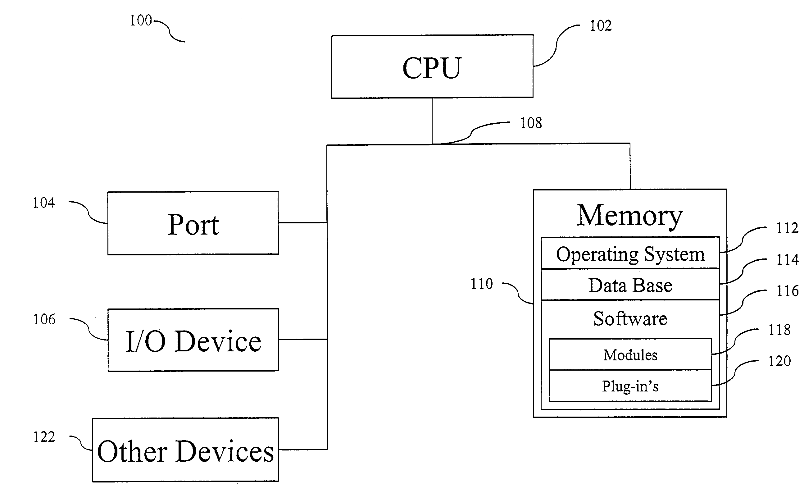
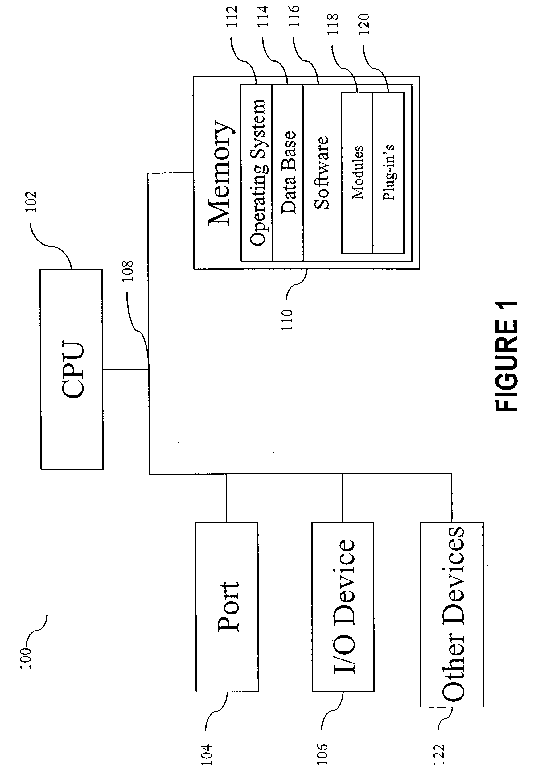
As shown in FIG. 1, system 100, according to one embodiment of the present invention, comprises a central processing unit (CPU) 102, which includes a RAM, and a disk memory 110 coupled to the CPU 102 through a bus 108. The system 100 further comprises a set of input / output (I / O) devices 106, such as a keypad, a mouse, and a display device, also coupled to the CPU 102 through the bus 108. The system 100 may further include an input port 104 for receiving data from a measurement device (not shown), as explained in more detail below. The system 100 may also include other devices 122. An example of system 100 is a Pentium 133 PC / Compatible computer having RAM larger than 64 MB and a hard disk larger than 1 GB.

Memory 110 has computer readable memory spaces such as database 114 that stores data, memory space 112 that stores operating system 112 such as Windows 95 / 98 / NT4.0 / 2000, which has instructions for communicating, processing, accessing, storing and searching data, and memory space...


PUM


Abstract

The present invention includes a method for modeling devices having different geometries, in which a range of interest for device geometrical variations is divided into a plurality of subregions each corresponding to a subrange of device geometrical variations. The plurality of subregions include a first type of subregions and a second type of subregions. The first or second type of subregions include one or more subregions. A regional global model is generated for each of the first type of subregions and a binning model is generated for each of the second type of subregions. The regional global model for a subregion uses one set of model parameters to comprehend the subrange of device geometrical variations corresponding to the G-type subregion. The binning model for a subregion includes binning parameters to provide continuity of the model parameters when device geometry varies across two different subregions.

Description

BACKGROUND OF THE INVENTION 1. Field of the Invention The invention relates generally to computer-aided electronic circuit simulation, and more particularly, to a method of extracting semiconductor device model parameters for use in integrated circuit simulation. 2. Description of Related Art While the sizes of individual devices have decreased, the complexities of integrated circuits have increased at a dramatic rate over the past few decades. As circuits have become more complex, traditional breadboard methods have become burdensome and overly complicated. Modern circuit designers rely more and more on computer aids, and electronic circuit simulators have become indispensable tools for circuit design. Examples of electronic circuit simulators include the Simulation Program with Integrated Circuit Emphasis (SPICE) developed at the University of California, Berkeley (UC Berkeley), and various enhanced versions or derivatives of SPICE, such as, SPICE2 or SPICE3, also developed at...

Claims


Application Information

Patent Timeline
Patent Type & Authority Applications(United States)
IPC IPC(8): G06F17/50
CPCG06F17/5036G06F30/367
Inventor CHEN, PINGLIU, ZHIHONG
Owner CADENCE DESIGN SYST INC
Why Eureka
Try Eureka