Method for forming programmable logic arrays using vertical gate transistors

a technology of vertical gate transistor and programmable logic array, which is applied in the field of integrated circuits, can solve the problems of large chip surface area, inability to solve the constraints placed on programmable logic array articles, and inability to meet the requirements of lithographic feature size and etc., to achieve the goal of overcoming the limit of the minimum lithographic feature size and the deficit in the available chip surface spa

Inactive Publication Date: 2005-02-10
MICRON TECH INC
View PDF42 Cites 18 Cited by
  • Summary
  • Abstract
  • Description
  • Claims
  • Application Information

AI Technical Summary

Benefits of technology

[0010] In one embodiment of the present invention, a novel programmable logic array is provided. The novel programmable logic array includes a plurality of input lines for receiving an input signal, a plurality of output lines, and one or more arrays having a first logic plane and a second logic plane connected between the input lines and the output lines. The first logic plane and the second logic plane comprise a plurality of logic cells arranged in rows and columns for providing a sum-of-products term on the output lines responsive to the received input signal. According to the teachings of the present invention, each logic cell includes a source region and a drain region in a horizontal substrate. A depletion mode

Problems solved by technology

Requiring a full MOSFET for each logic input consumes a significant amount of chip surface area.
However, all of these studies and articles on pass transistor logic have not provided a solution to the constraints placed on programmable logic arrays by the limits of the minimum lithographic featur

Method used


Image

  • Method for forming programmable logic arrays using vertical gate transistors
  • Method for forming programmable logic arrays using vertical gate transistors
  • Method for forming programmable logic arrays using vertical gate transistors

Examples


Embodiment Construction

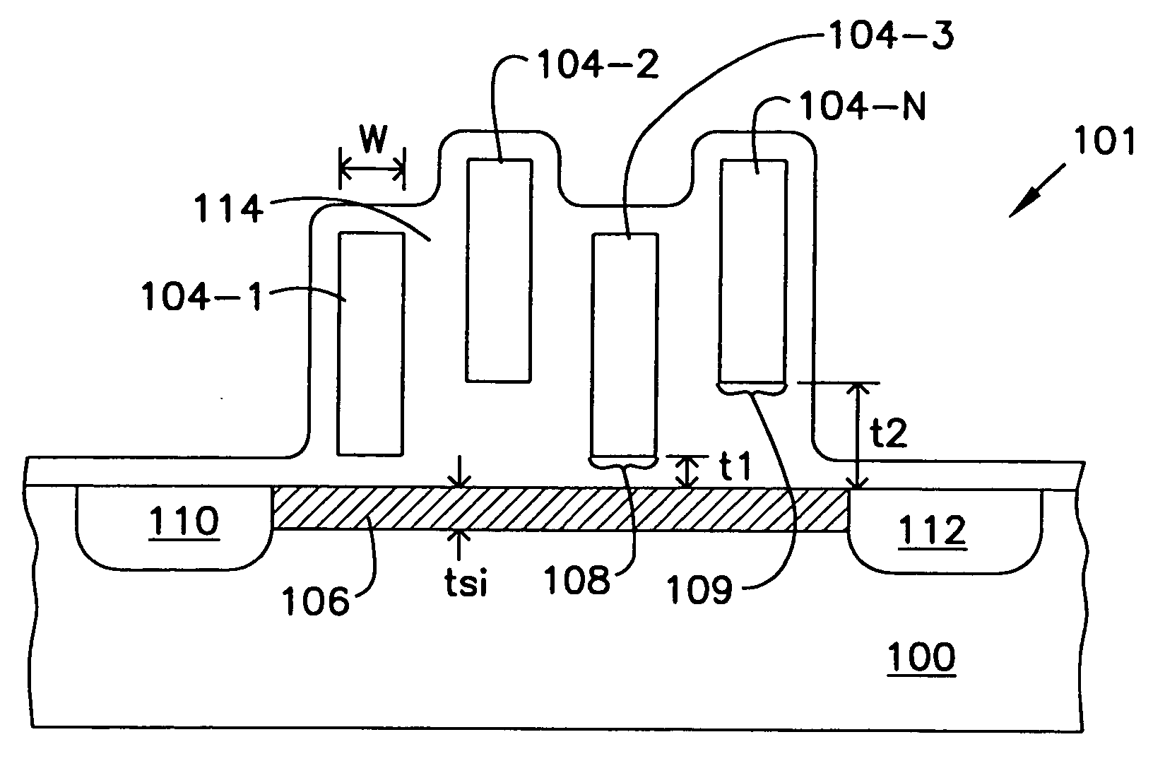
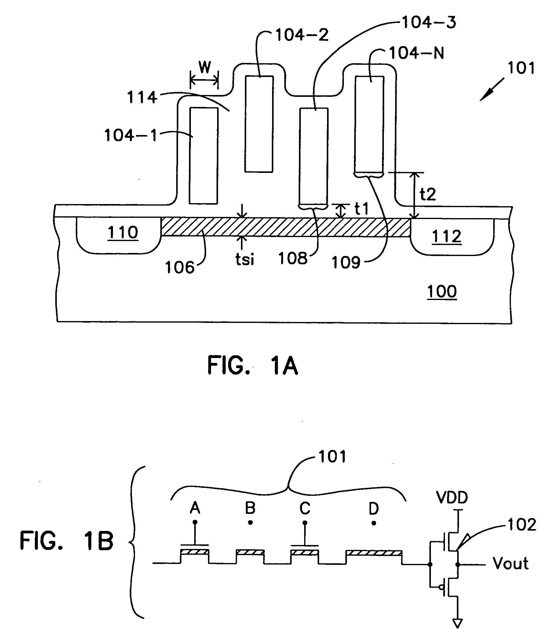
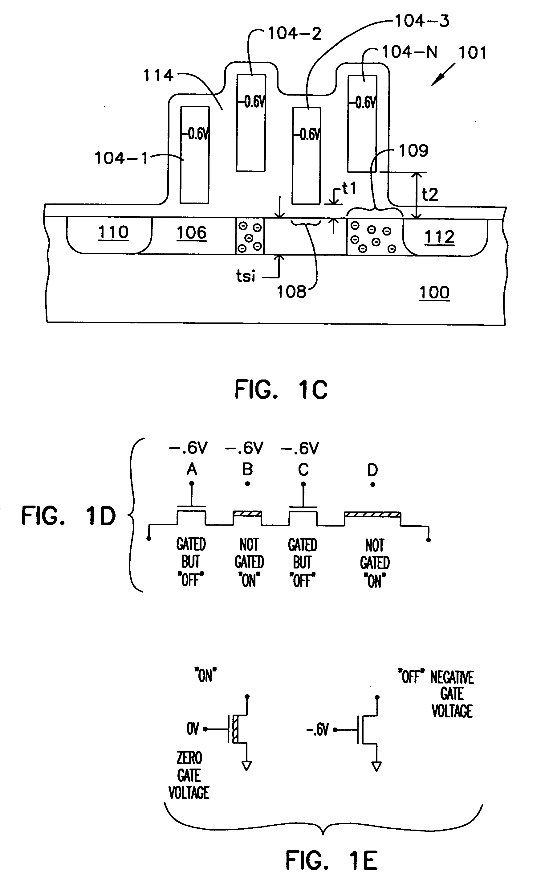
[0032] In the following detailed description of the invention, reference is made to the accompanying drawings which form a part hereof, and in which is shown, by way of illustration, specific embodiments in which the invention may be practiced. In the drawings, like numerals describe substantially similar components throughout the several views. These embodiments are described in sufficient detail to enable those skilled in the art to practice the invention. Other embodiments may be utilized and structural, logical, and electrical changes may be made without departing from the scope of the present invention. The terms wafer and substrate used in the following description include any structure having an exposed surface with which to form the integrated circuit (IC) structure of the invention. The term substrate is understood to include semiconductor wafers. The term substrate is also used to refer to semiconductor structures during processing, and may include other layers that have b...


PUM


Abstract

One aspect disclosed herein relates to a method for forming a programmable logic array. Various embodiments of the method include forming a first logic plane and a second logic plane, each including a plurality of logic cells interconnected to implement a logical function. Forming the logic cells includes forming a horizontal substrate with a source region, a drain region, and a depletion mode channel region separating the source and the drain regions, and further includes forming a number of vertical gates located above different portions of the depletion mode channel region. At least one vertical gate is separated from the depletion mode channel region by a first oxide thickness, and at least one of the vertical gates is separated from the depletion mode channel region by a second oxide thickness. Other aspects and embodiments are provided herein.

Description

CROSS REFERENCE TO RELATED APPLICATIONS [0001] This application is a Divisional of U.S. Ser. No. 10 / 185,155 filed Jun. 28, 2002, which is a Divisional of U.S. Ser. No. 09 / 643,296 filed on Aug. 22, 2000, now issued as U.S. Pat. No. 6,437,389, which applications are incorporated herein by reference. [0002] This application is related to the following co-pending, commonly assigned U.S. patent applications: entitled “Static Pass Transistor Logic with Transistors with Multiple Vertical Gates,” Ser. No. 09 / 580,901; and “Vertical Gate Transistors in Pass Transistor Logic Decode Circuits,” Ser. No. 09 / 580,860, both filed on May 30, 2000 and which disclosures are herein incorporated by reference.TECHNICAL FIELD OF THE INVENTION [0003] This invention relates generally to integrated circuits and in particular to vertical gate transistors in pass transistor programmable logic arrays. BACKGROUND OF THE INVENTION [0004] Many programmable logic arrays include multiple transistors arrayed such that...

Claims


Application Information

Patent Timeline
IPC IPC(8): H01L21/336H01L21/8246H01L27/112H01L27/118H01L29/423H01L29/78H01L31/072
CPCH01L27/112H01L27/11233H01L27/11803H01L29/7831H01L29/42368H01L29/66484H01L29/42324H10B20/36H10B20/00
Inventor FORBES, LEONARDAHN, KIE Y.
Owner MICRON TECH INC
Why Eureka
Try Eureka