Multiple-gate transistors formed on bulk substrates

Active Publication Date: 2005-02-17
TAIWAN SEMICON MFG CO LTD
View PDF14 Cites 220 Cited by
  • Summary
  • Abstract
  • Description
  • Claims
  • Application Information

AI Technical Summary

Benefits of technology

[0012] The preferred embodiment of the present invention provides a multiple-gate transistor that is formed on a bulk substrate. Bulk silicon substrates are cheaper than silicon-on-ins

Problems solved by technology

Consequently, a transistor with a short gate length suffers from problems related to the inability of the gate to substantially control the on and off states of the channel.
However, for device scaling well into the sub-50 nm regime,

Method used


Image

  • Multiple-gate transistors formed on bulk substrates
  • Multiple-gate transistors formed on bulk substrates
  • Multiple-gate transistors formed on bulk substrates

Examples


Embodiment Construction

[0029] The making and using of the presently preferred embodiments are discussed in detail below. It should be appreciated, however, that the present invention provides many applicable inventive concepts that can be embodied in a wide variety of specific contexts. The specific embodiments discussed are merely illustrative of specific ways to make and use the invention, and do not limit the scope of the invention.

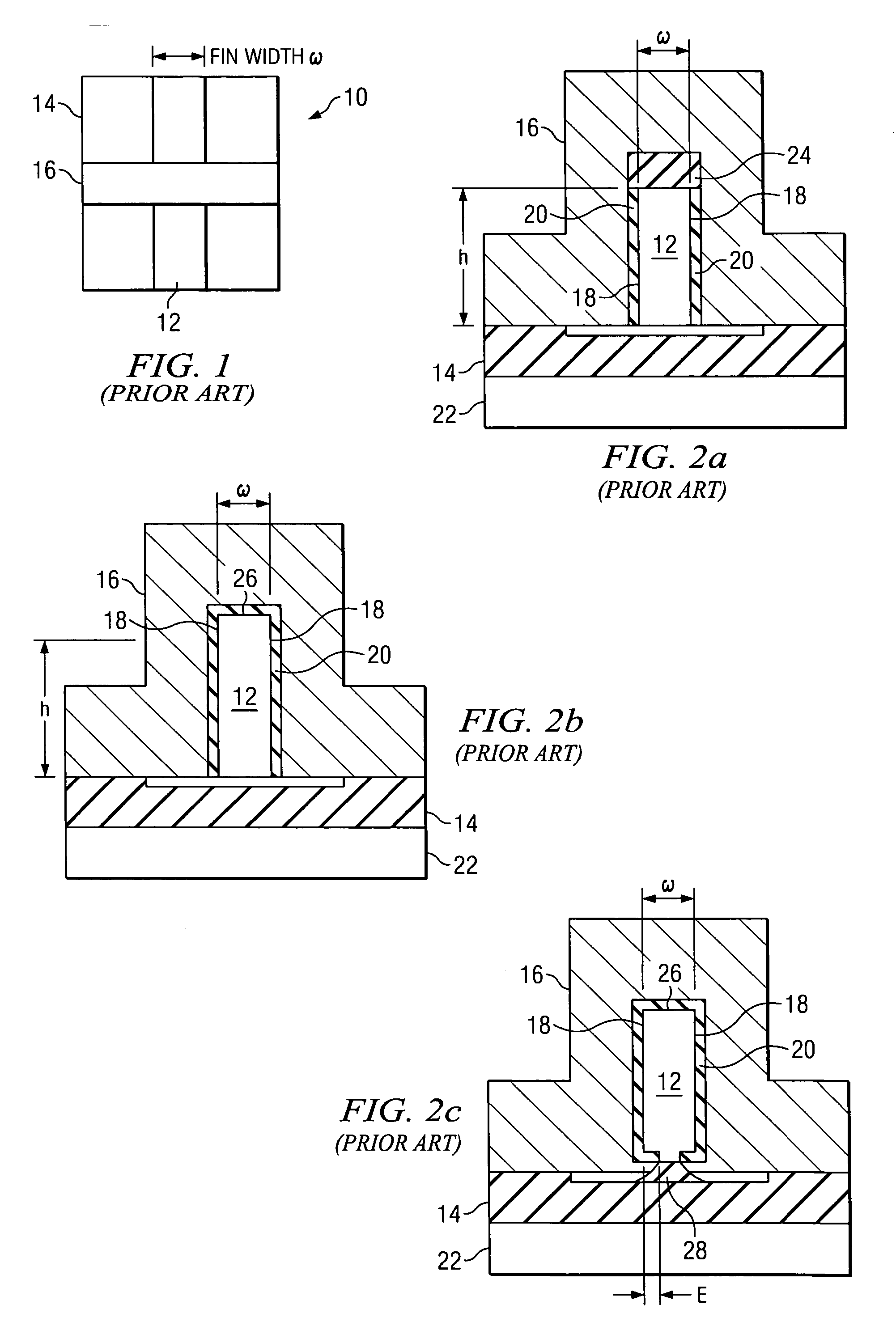
[0030] The preferred embodiment relates to the field of semiconductor devices and more particularly to semiconductor devices with multiple gates. Aspects of this invention provide a structure and method for forming multiple-gate transistors on bulk silicon substrates.

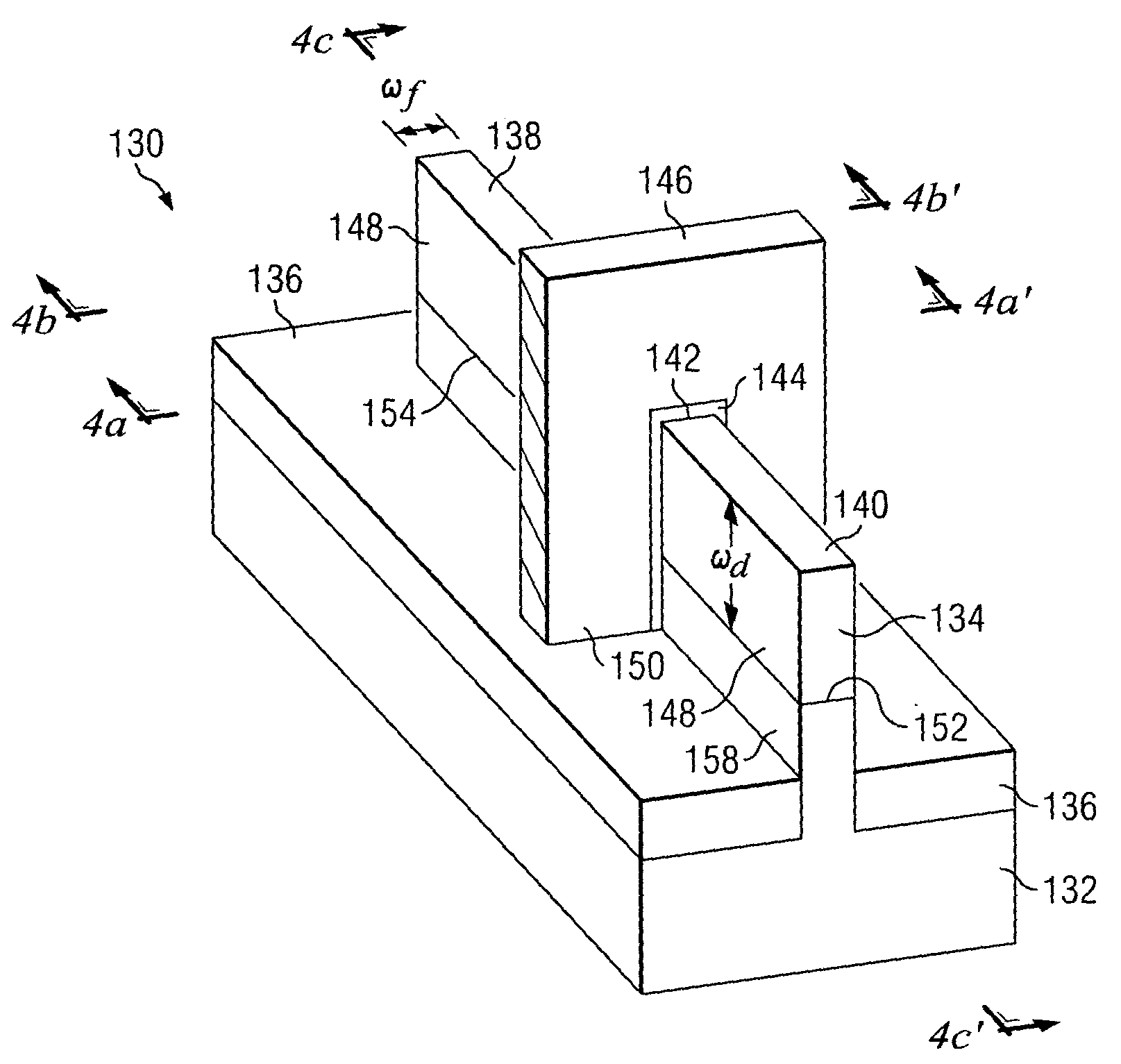
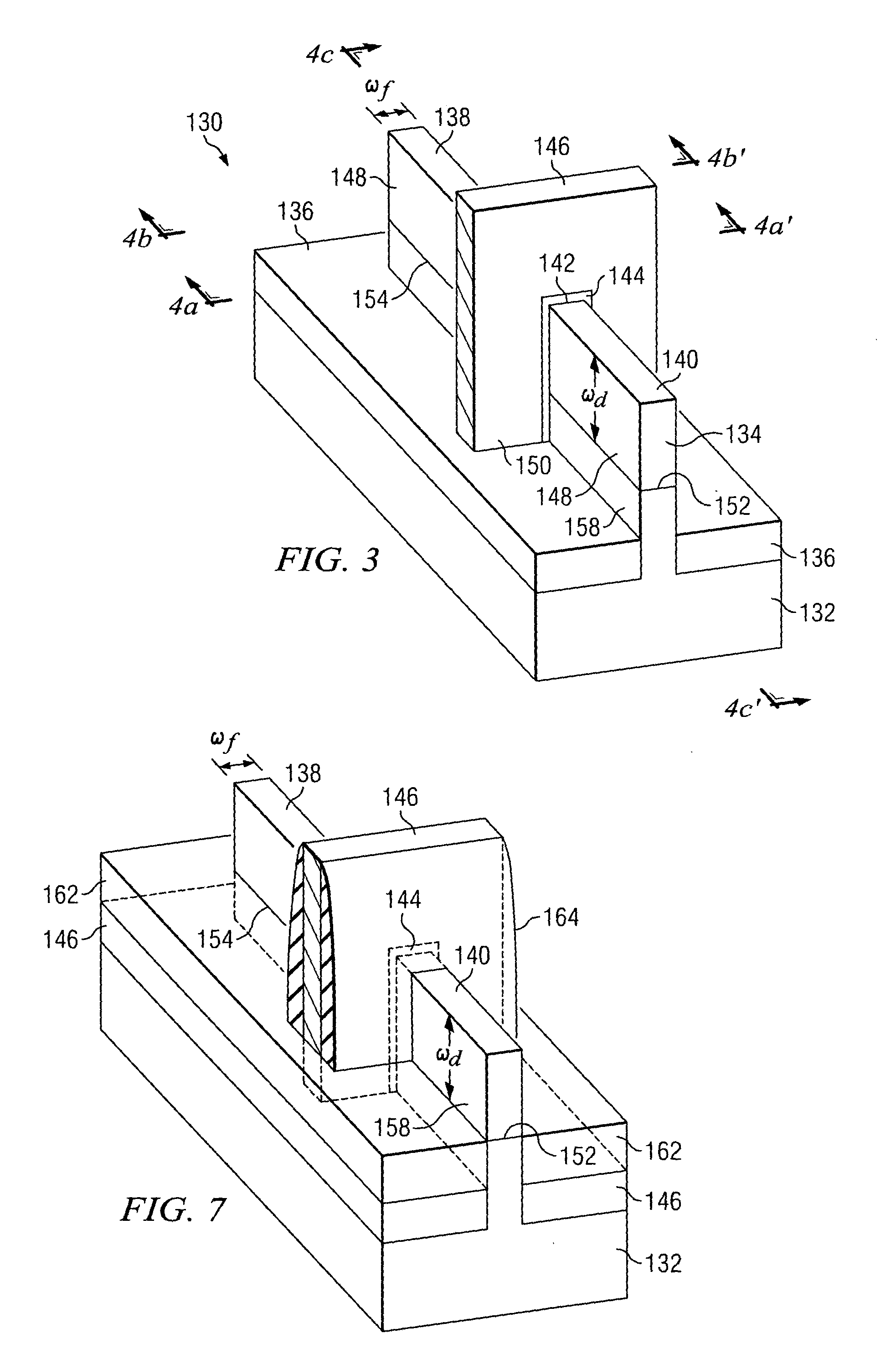
[0031]FIG. 3 shows a three-dimensional perspective of a triple-gate transistor 130 formed on a bulk substrate 132 according to a first embodiment of this invention. The substrate 132 material can be any semiconductor material. For example, the substrate 132 can be an elemental semiconductor such as silicon or ...


PUM


Abstract

In one aspect, the present invention teaches a multiple-gate transistor 130 that includes a semiconductor fin 134 formed in a portion of a bulk semiconductor substrate 132. A gate dielectric 144 overlies a portion of the semiconductor fin 134 and a gate electrode 146 overlies the gate dielectric 144. A source region 138 and a drain region 140 are formed in the semiconductor fin 134 oppositely adjacent the gate electrode 144. In the preferred embodiment, the bottom surface 150 of the gate electrode 146 is lower than either the source-substrate junction 154 or the drain-substrate junction 152.

Description

[0001] This application claims the benefit of U.S. Provisional Application No. 60 / 495,071, filed on Aug. 13, 2003, entitled “Multiple-Gate Transistors Formed on Bulk Substrates,” which application is hereby incorporated herein by reference.TECHNICAL FIELD [0002] The present invention relates to semiconductor devices and more particularly to the multiple-gate transistors formed on bulk semiconductor substrates. BACKGROUND [0003] The dominant semiconductor technology used for the manufacture of ultra-large scale integrated (ULSI) circuits is the metal-oxide-semiconductor field effect transistor (MOSFET) technology. Reduction in the size of MOSFETs has provided continued improvement in speed performance, circuit density, and cost per unit function over the past few decades. As the gate length of the conventional bulk MOSFET is reduced, however, the source and drain increasingly interact with the channel and gain influence on the channel potential. Consequently, a transistor with a shor...

Claims


Application Information

Patent Timeline
IPC IPC(8): H01L21/00H01L21/336H01L21/8234H01L29/76H01L29/78H01L29/786
CPCH01L29/66628H01L29/66795H01L2029/7857H01L29/7851H01L29/7853H01L29/66818
Inventor YEO, YEE-CHIAYANG, FU-LIANGHU, CHENMING
Owner TAIWAN SEMICON MFG CO LTD
Why Eureka
Try Eureka