
Solid state imaging device, driving method therefor, and imaging apparatus

a solid-state imaging and driving method technology, applied in the direction of radio frequency controlled devices, television systems, instruments, etc., can solve the problems of serious deterioration of image quality, insufficient display of advantages of progressive scan systems, and increased aliasing noise and aliasing signals, so as to reduce the time required for vertical transfer operation and improve the frame rate of solid-state imaging devices

Inactive Publication Date: 2005-02-17
SONY CORP
View PDF11 Cites 29 Cited by
  • Summary
  • Abstract
  • Description
  • Claims
  • Application Information

AI Technical Summary

Benefits of technology

[0011] According to the progressive-scan-system solid-state imaging device of the present invention, electric charges for a plurality of pixels in the vertical direction can be added without a time difference. Thus, in the progressive scan system, high-definition images can be obtained without a time difference. Additionally, the time required for a vertical transfer operation can be decreased, and the frame rate of the solid-state imaging device can be improved.

Problems solved by technology

For moving pictures, if a decimation function is merely added to a multi-pixel solid-state imaging device, aliasing noise and aliasing signals are increased, and the image quality is seriously deteriorated.
In this case, however, after reading odd-numbered lines, if the quantity of incident light considerably changes before reading even-numbered lines, such a change is reflected in a resulting image, and thus, advantages of the progressive scan system cannot be sufficiently exhibited.

Method used


Image

  • Solid state imaging device, driving method therefor, and imaging apparatus
  • Solid state imaging device, driving method therefor, and imaging apparatus
  • Solid state imaging device, driving method therefor, and imaging apparatus

Examples


Embodiment Construction

[0017] The present invention is described in detail below with reference to the accompanying drawings through illustration of an embodiment.

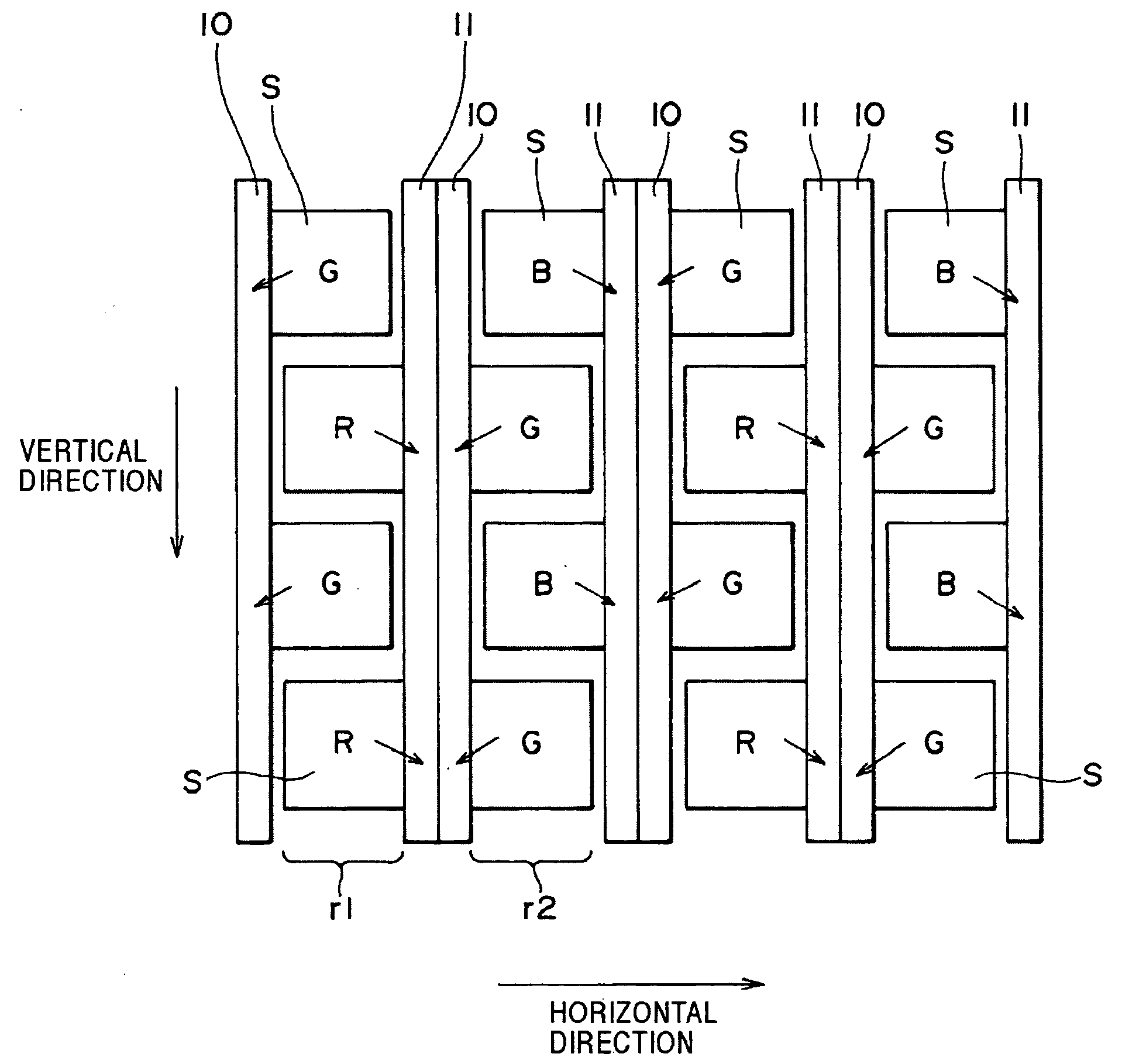
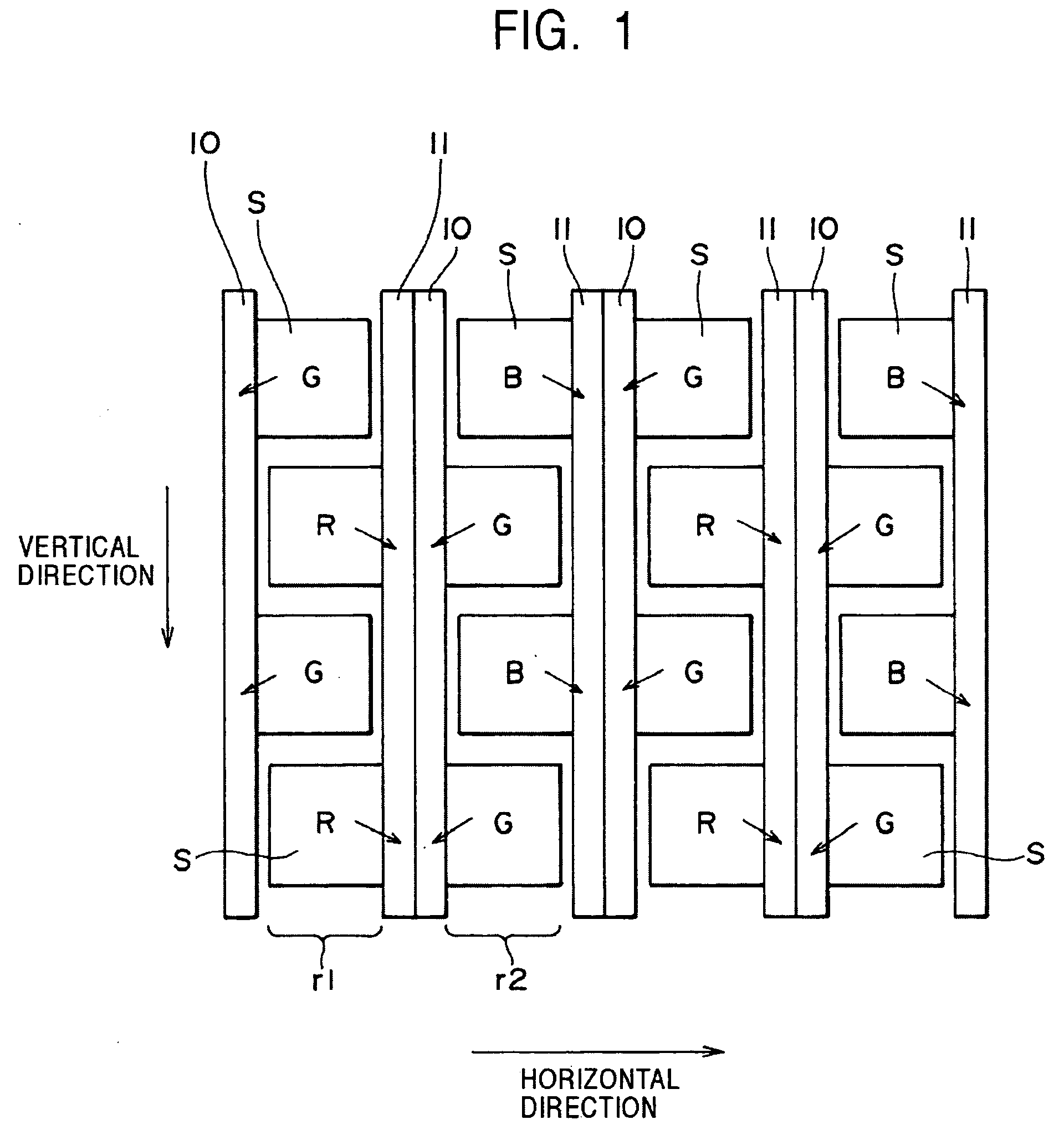
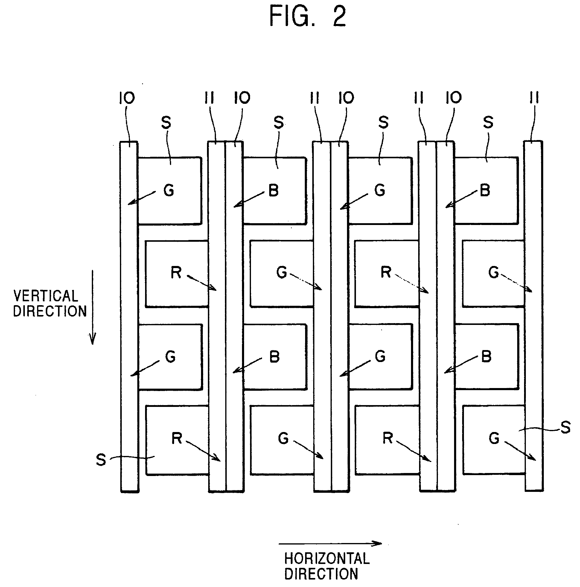
[0018] A solid-state imaging device constructed in accordance with an embodiment of the present invention shown in FIG. 1 includes sensor areas in which a plurality of pixel sensors S are disposed in the horizontal and vertical directions, and two vertical transfer portions 10 and 11 disposed at the two sides of each pixel column, which is formed of the plurality vertical pixel sensors S.

[0019] With this configuration, the reading and transferring of electric charges stored in the pixel sensors S is controlled by a controller (not shown). In this embodiment, electric charges stored in adjacent pixel sensors S in the vertical direction in each pixel column are read in different directions by the two vertical transfer portions 10 and 11. Then, electric charges read from the plurality of pixel sensors S are added and transferred in each of the ve...


PUM


Abstract

A solid-state imaging device includes sensor areas, in each of the sensor areas, a plurality of pixel sensors are disposed in the vertical direction and in the horizontal direction. Two vertical transfer portions are formed across each pixel column including the plurality of pixel sensors in the vertical direction. A controller controls electric charges stored in the pixel sensors vertically adjacent to each other in each pixel column to be simultaneously read in different directions by the two vertical transfer portions, and also controls each of the two vertical transfer portions to add and transfer electric charges for the plurality of pixel sensors. With this configuration, the time required for a vertical transfer operation can be decreased, and the frame rate of the solid-state imaging device can be improved.

Description

BACKGROUND OF THE INVENTION [0001] 1. Field of the Invention [0002] The present invention relates to a progressive-scan-system solid-state imaging device and a driving method therefor for simultaneously reading electric charges stored in a plurality of pixel sensors that are disposed in a matrix in the horizontal and vertical directions. The present invention also relates to an imaging apparatus, for example, a digital still camera or a digital video camera, including an optical system, such as a lens, an image signal processor, and a recording medium. In the imaging apparatus, an image is read by using the solid-state imaging device through the optical system, undergoes predetermined signal processing, and is then recorded on the recording medium. [0003] 2. Description of the Related Art [0004] Due to the versatility of functions of solid-state imaging devices, it is demanded that solid-state imaging devices used for digital still cameras achieve a multi-pixel output and a high fra...

Claims


Application Information

Patent Timeline
IPC IPC(8): H01L27/148G09G3/20H01L27/14H01L27/146H01L31/10H04N5/335H04N5/341H04N5/347H04N5/372H04N9/04H04N9/07
CPCH04N3/1537H04N9/07H04N9/045H04N25/46H04N25/73H04N23/12H01L27/146H01L31/10
Inventor KIMURA, MASAO
Owner SONY CORP
Learn More