Deep filled vias

a technology of conductive vias and deep filling, which is applied in the direction of basic electric elements, semiconductor/solid-state device manufacturing, electric apparatus, etc., can solve the problems of increasing resistivity, electrical failure of devices, and difficulty in obtaining reproducibly acceptable vias within chips and from batch to batch

Active Publication Date: 2005-02-17
GLOBALFOUNDRIES US INC
View PDF25 Cites 79 Cited by
  • Summary
  • Abstract
  • Description
  • Claims
  • Application Information

AI Technical Summary

Benefits of technology

[0015] The present invention is directed to filled deep conductive vias, and the process of making filled deep conductive vias, in which the aspect ratio is greater than about 2. Although equivalent aspect ratios have been successfully electroplated in vias having smaller dimensions, the high aspect ratios seen for voidless copper plated vias of the present invention have not been fabricated heretofore for such depths nor under the same process conditions. The upper limit of the aspect ratio in a blind via is dependent only on the thickness of the material within which the via is to be situated and the amount of material required to remain below the via in order to maintain structura

Problems solved by technology

Stresses caused by such irregularities contribute to electromigration problems, increased resistivity of the via, ultimately the electrical failure of the device and difficulty in obtaining reproducibly acceptable vias within a chip and from batch to batch.
Resistivity limits signal speed.
However, as the diameter of interlevel vias in ICs approach one micron (μm) or less and aspect ratios approach 1 or more, sloping alone does not provide consistently satisfactory coverage.
In addition, since sloping involves widening at the via opening, it uses up valuable real estate and increases the pitc

Method used


Image

  • Deep filled vias
  • Deep filled vias
  • Deep filled vias

Examples


Embodiment Construction

[0024] In order to facilitate understanding of the present invention, reference is made to the following detailed description taken in conjunction with FIGS. 1a-4c.

[0025] Fabricating Deep Vias

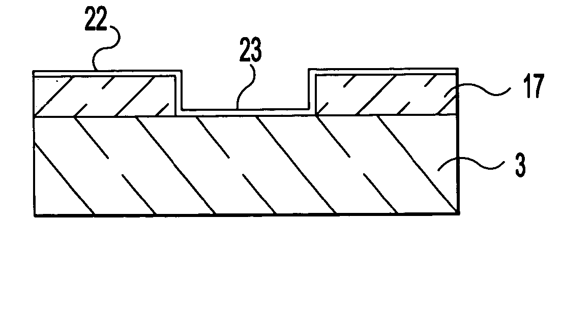
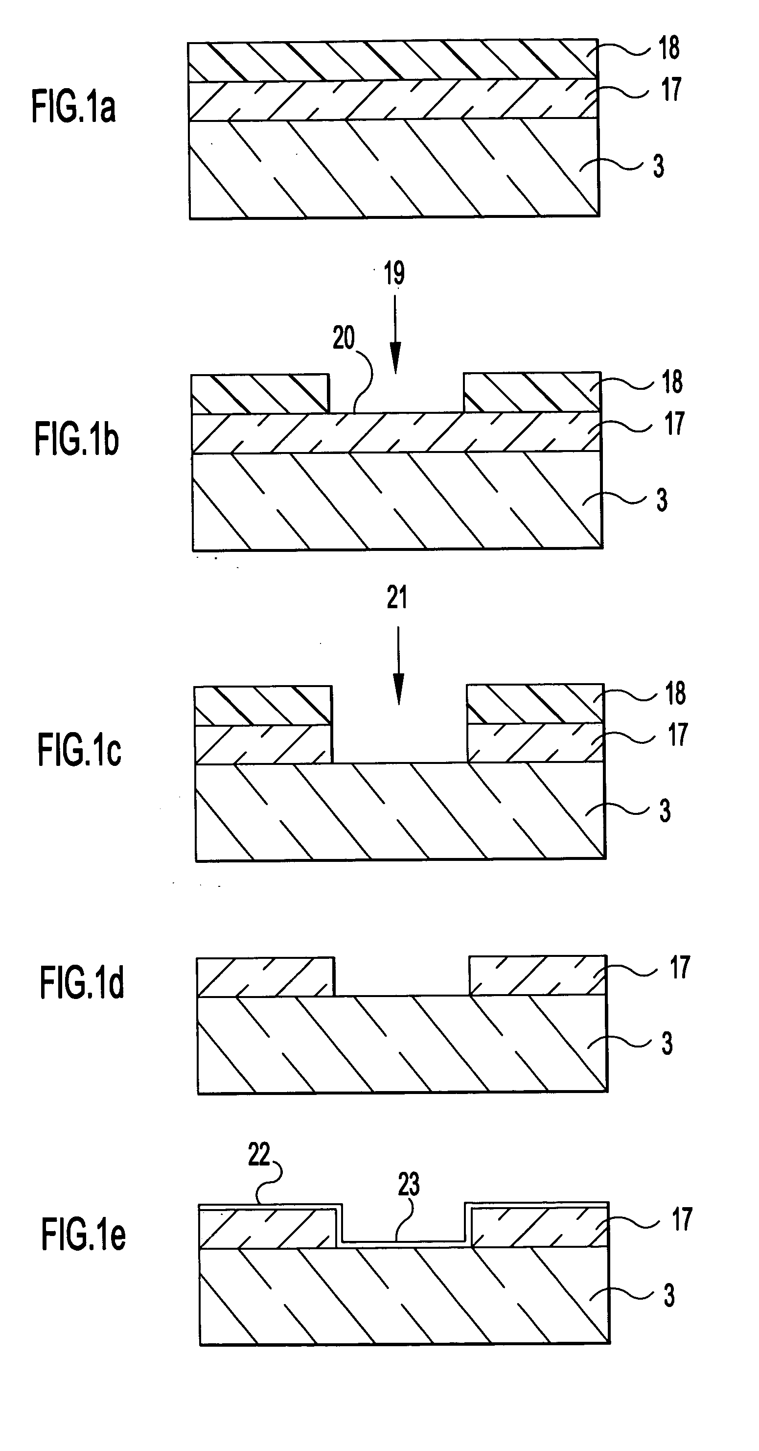
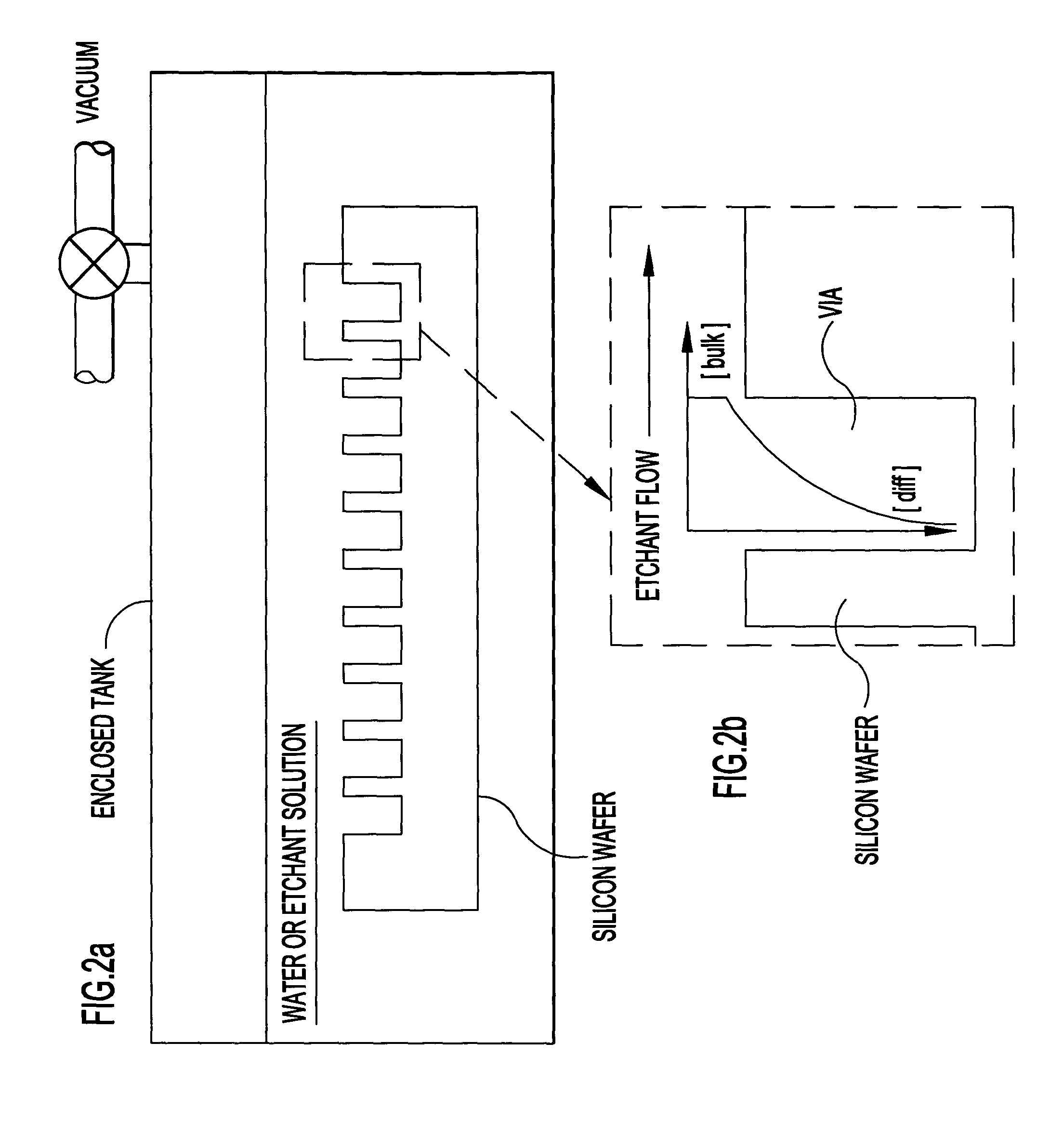
[0026] In FIGS. 1a-1e and 3a, sequences for forming a filled blind via structure are depicted. In FIG. 3a, an unflared deep via structure option is shown, and in FIG. 3b a preferred flared deep via structure option is shown. The vias, shown in the 2-dimensional drawings as U-shaped, are formed within material 3, which typically comprises silicon. Deep vias in FIGS. 3a and 3b extend from an upper surface 4 of material 3 down to bottom surface 5, a via depth of 6. In the presently preferred embodiment, depth 6 is between about 100 μm and about 300 μm, and more preferably is about 200 μm. Most preferably, vias in FIGS. 3a and 3b may extend through the entire vertical thickness 7 of material 3 to lower surface 8 of material 3, which is interfaced with the upper surface of substrate material 9. Ma...


PUM


Abstract

Flared and non-flared metallized deep vias having aspect ratios of about 2 or greater are provided. Blind vias have been fabricated in silicon substrates up to a depth of about 300 microns, and flared through vias have been fabricated up to about 750 microns, the approximate thickness of a silicon substrate wafer, enabling the formation of electrical connections at either or both ends of a via. In spite of the depth and high aspect ratios attainable, the etched vias are completely filled with plated copper conductor, completing the formation of deep vias and allowing fuller use of both sides of the substrate.

Description

BACKGROUND OF THE INVENTION [0001] The present invention relates to the formation of metallized, high aspect ratio vias, in which the diameter at least one of two ends of a via is preferably flared, the ends being connected by side walls therebetween. More particularly, the present invention relates to high aspect ratio plated conductive vias which are fabricated in the semiconductor substrate of a multichip module (CM) or packaging structure. Other applications include, but are not limited to, micro-electro-mechanical systems (MEMs); micro-opto-electro-mechanical systems (MOEMs); RF MEMs; BioMEMs; lab-on-chip (LOC) and other sensors; and membranes. [0002] Much work has been done in the integrated circuit (IC) art to address reliability problems in metallized vias attributed to poor metal coverage of via side walls, lower step coverage at angularities such as at via and wiring level intersections, metal flaking at stress points, and incomplete fill of metal within the via. Stresses ...

Claims


Application Information

Patent Timeline
IPC IPC(8): H01L21/288H01L21/3065H01L21/4763H01L21/768
CPCH01L21/2885H01L21/76898H01L21/30655
Inventor ANDRICACOS, PANAYOTISCOOPER, EMANUEL ISRAELDALTON, TIMOTHY JOSEPHDELIGIANNI, HARIKLIAGUIDOTTI, DANIELKWIETNIAK, KEITH THOMASSTEEN, MICHELLE LEIGHTSANG, CORNELIA KANG-I
Owner GLOBALFOUNDRIES US INC
Why Eureka
Try Eureka