Memory testing apparatus and method

a technology of memory and testing apparatus, applied in the direction of wireless architecture, semiconductor/solid-state device testing/measurement, instruments, etc., can solve the problems of increasing the time and expense required to perform such operational margin test on the predetermined memory, increasing the time and expense required to count the detected failures, and requiring a certain amount of time to compl

Active Publication Date: 2005-02-24
SAMSUNG ELECTRONICS CO LTD
View PDF10 Cites 15 Cited by
  • Summary
  • Abstract
  • Description
  • Claims
  • Application Information

AI Technical Summary

Benefits of technology

The present invention provides an exemplary memory testing apparatus and method for operating such an apparatus, that can reduce the time required to test a memory from that required using the conventional memory testing apparatus and methods.

Problems solved by technology

with each of the operations requiring a certain amount of time to complete.
However, as the storage capacity of the memory devices being tested increases, the time and expense required to perform such operational margin tests on the predetermined memory and count the detected failures also increases.

Method used


Image

  • Memory testing apparatus and method
  • Memory testing apparatus and method
  • Memory testing apparatus and method

Examples


Embodiment Construction

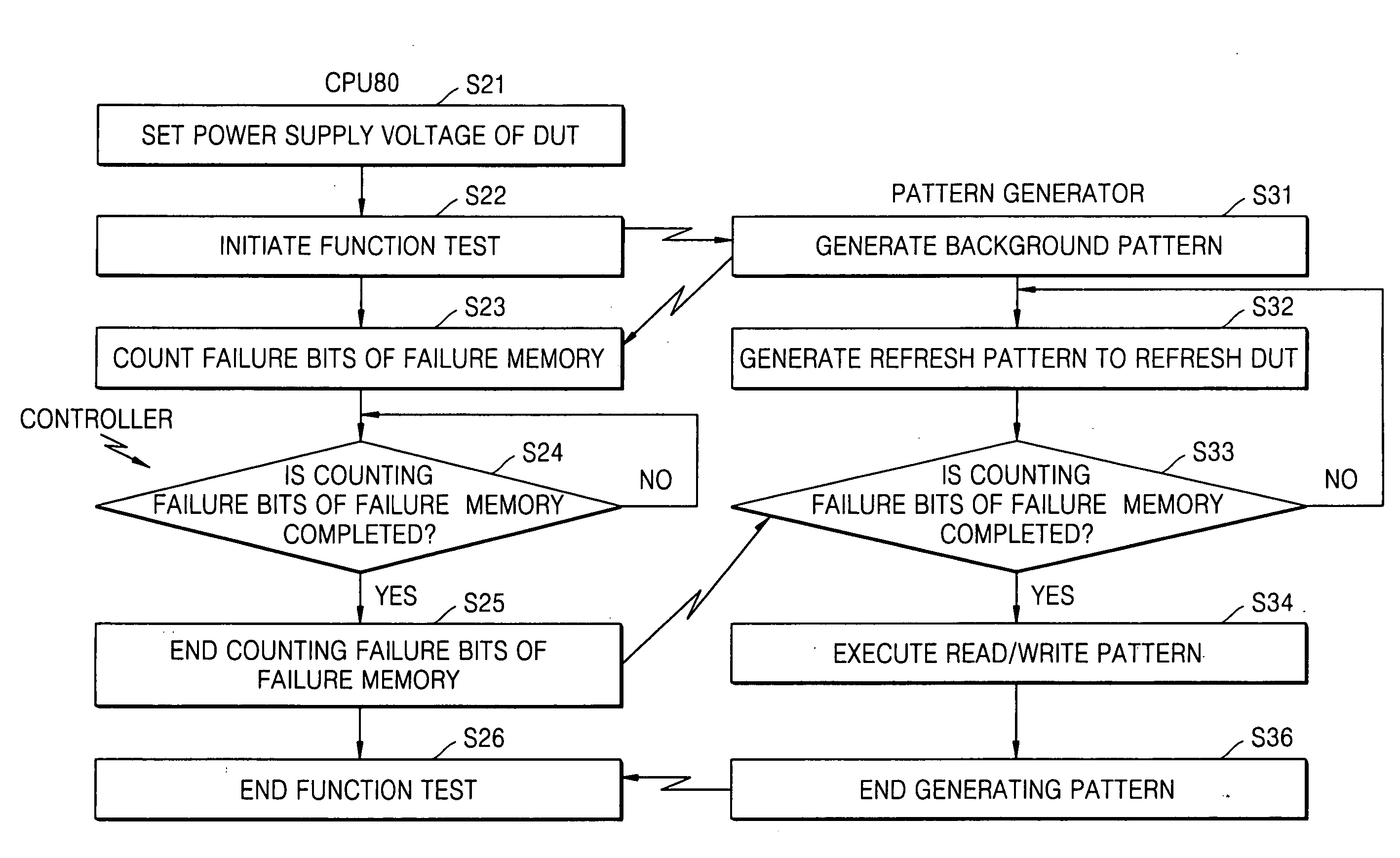
The present invention will now be described more fully with reference to the accompanying drawings, in which exemplary embodiments of the invention are shown. FIG. 3 is a block diagram of a memory testing apparatus according to an exemplary embodiment of the present invention. In FIGS. 1, 3 and 5, corresponding reference numerals indicate corresponding, if not identical, elements whose descriptions will not be repeated for the sake of brevity.

Referring to FIG. 3, a pattern generator 20, which generally corresponds to the pattern generator 2 of FIG. 1, generates a background pattern to be applied to a memory (hereinafter referred to as a device under test (DUT)) 10 and outputs a count starting signal C′. In addition, the pattern generator 20 generates test patterns, i.e., read / write test patterns, and addresses and outputs the test patterns to the DUT 10 when it receives a count ending signal D′. The pattern generator 20 includes a background pattern commanding unit 21 and a test ...


PUM


Abstract

Provided are a memory device testing apparatus and method of operating such an apparatus that can reduce the time required to test a memory device such as a DRAM. The memory testing apparatus includes a pattern generator, a test head, an address pointer, a selector, a failure memory, a failure bit counter and a controller for coordinating the operation of the various elements. Depending on the signals received from the controller, the pattern generator will generate background pattern(s) or test patterns and address information that are, in turn, output to the memory device under test and the selector. During funtional testing of the memory device, failure data is accumulated in a failure memory and subsequently output to a failure bit counter using address information from the address pointer while the background or test pattern is being written to the memory device.

Description

CROSS-REFERENCE TO RELATED APPLICATIONS This application claims priority from Japanese Patent Application No. 2003-146319, which was filed on May 23, 2003, in the Japanese Patent Office, the disclosure of which is incorporated herein in its entirety by reference. BACKGROUND OF THE INVENTION 1. Field of the Invention The present invention relates to a memory testing apparatus and testing method in which the test results corresponding to the performance of a memory under test are stored in a failure memory and subsequently counting the failure bits stored in the failure memory, and more particularly, to a memory testing apparatus and method, which can reduce the time required for functional testing of memory devices. 2. Description of the Related Art Memory testing apparatuses perform tests for various operational parameters of a memory, such as a power supply voltage margin and access time, and count defective bits of the memory. A conventional memory testing apparatus, such as ...

Claims


Application Information

Patent Timeline
Patent Type & Authority Applications(United States)
IPC IPC(8): G01R31/28G01R31/3183G11C29/00G11C29/56H01L21/66
CPCG11C29/56G11C2029/1208G11C29/56004H04Q9/00G08C17/02H04Q2209/40G08C2201/93
Inventor KANG, KI-SANGAKIYAMA, TSUTOMUPARK, JE-YOUNG
Owner SAMSUNG ELECTRONICS CO LTD
Why Eureka
Try Eureka