Method of fabricating electronic component using resist structure with no undercut

a resist structure and electronic component technology, applied in nanoinformatics, instruments, record information storage, etc., can solve the problems of increasing sensor resistance, unable to reliably perform a trackwidth below 130 nm, and reaching the limit of the bilayer resist process

Inactive Publication Date: 2005-03-03
WESTERN DIGITAL TECH INC
View PDF6 Cites 12 Cited by
  • Summary
  • Abstract
  • Description
  • Claims
  • Application Information

AI Technical Summary

Problems solved by technology

However, as the sensor trackwidths have decreased with product and technology roadmaps, the bilayer resist process has reached its limits.
It cannot be performed reliably for trackwidths below 130 nm, mainly because the width of the photoresist underlayer becomes too small to support the overlayer.
This unwanted material creates a large physical separation between the read sensor and its stabilization (HB) layer, resulting in increased sensor resistance and poor magnetic stability.
The increased separation translates into free layer instability.
Another problem is that fencing causes a flaring of the gap.
The result is that the sensor has a much different magnetic proportion than the design ideals, leading to inferior performance.

Method used


Image

  • Method of fabricating electronic component using resist structure with no undercut
  • Method of fabricating electronic component using resist structure with no undercut
  • Method of fabricating electronic component using resist structure with no undercut

Examples


Embodiment Construction

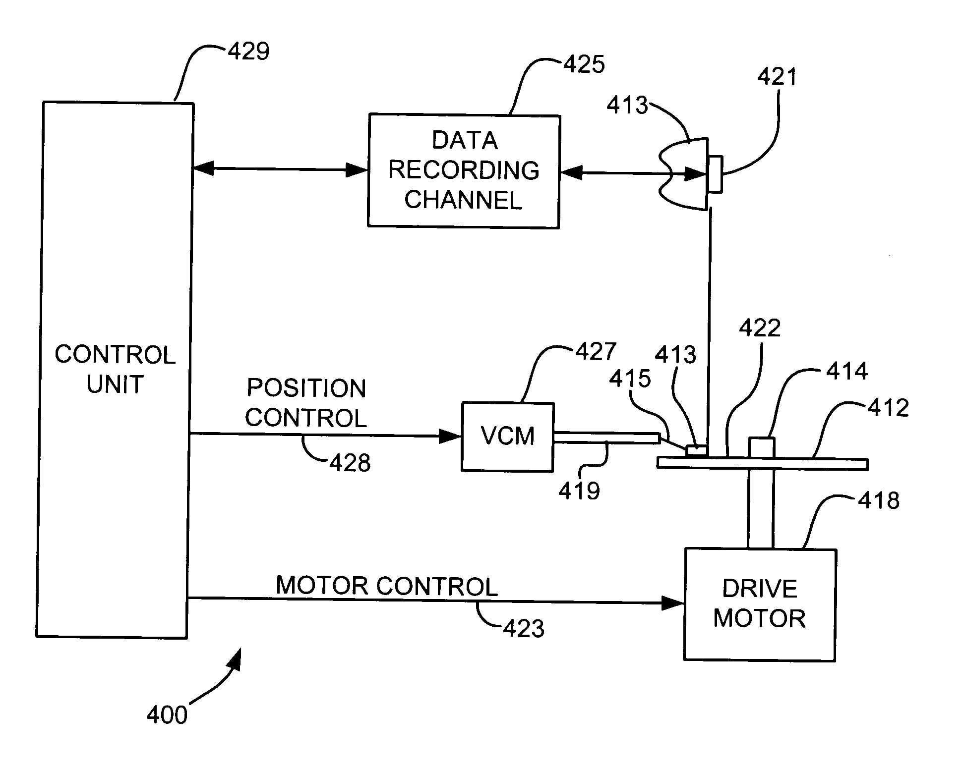
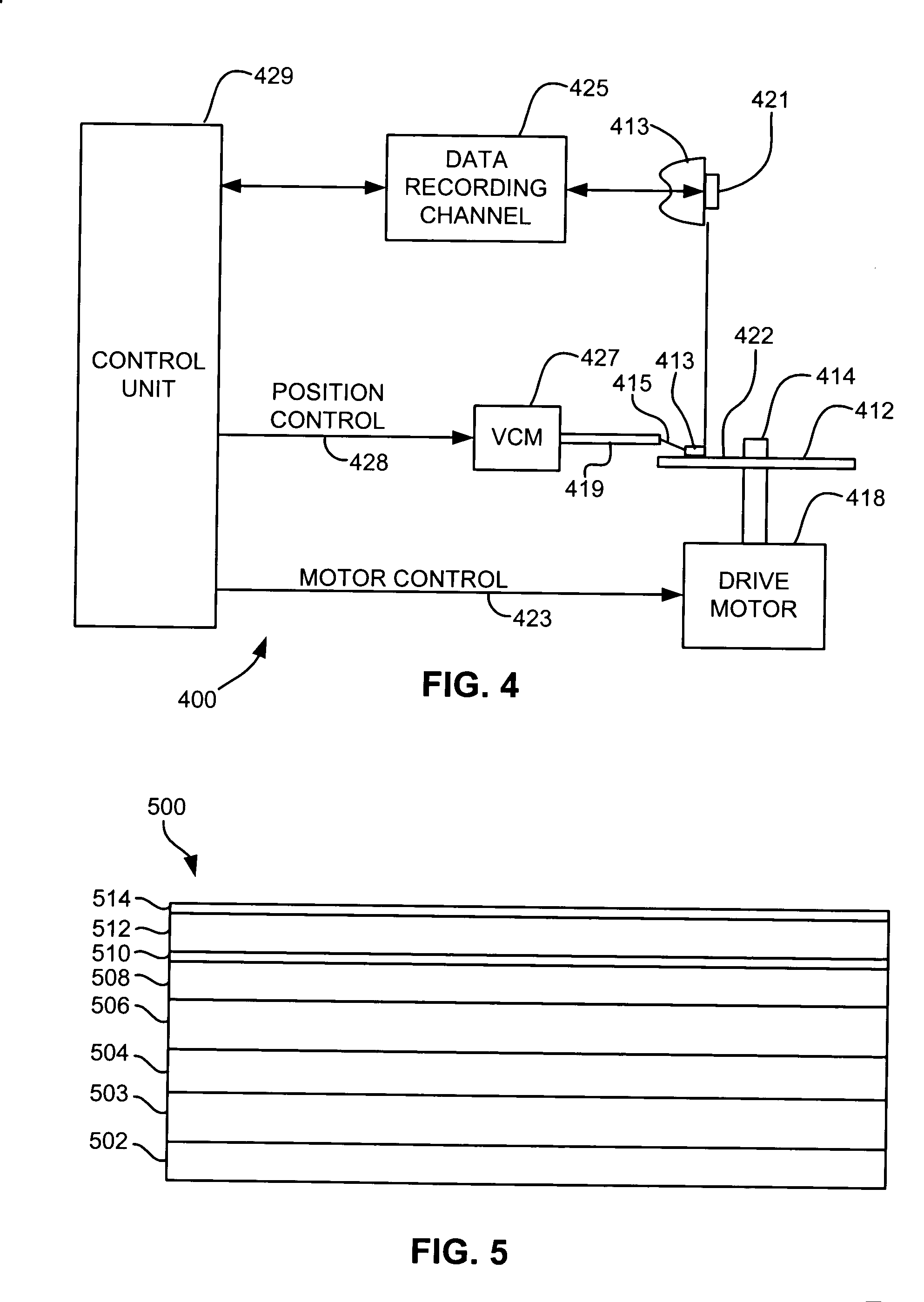
[0026] The following description is the best embodiment presently contemplated for carrying out the present invention. This description is made for the purpose of illustrating the general principles of the present invention and is not meant to limit the inventive concepts claimed herein.

[0027] Referring now to FIG. 4, there is shown a disk drive 400 embodying the present invention. As shown in FIG. 4, at least one rotatable magnetic disk 412 is supported on a spindle 414 and rotated by a disk drive motor 418. The magnetic recording media on each disk is in the form of an annular pattern of concentric data tracks (not shown) on disk 412.

[0028] At least one slider 413 is positioned adjacent to the disk 412, each slider 413 supporting one or more magnetic read / write heads 421. More information regarding such heads 421 will be set forth hereinafter during reference to the remaining FIGS. As the disks rotate, slider 413 is moved radially in and out over disk surface 422 so that heads 4...


PUM

PropertyMeasurementUnit
incidence angleaaaaaaaaaa
widthaaaaaaaaaa
structureaaaaaaaaaa

Abstract

A method for milling a structure. A single- or multi-layer resist having no undercut is added to a surface of a structure to be milled, the surface to be milled defining a plane. A milling process, such as ion milling, is performed. The milling process includes milling the structure at high incidence and milling the structure at razing incidence. The milling process can be performed only once, or repeated multiple times. High incidence can be defined as about 65 to about 90 degrees from the plane of the surface being milled. Razing incidence can be defined as about 0 to about 30 degrees from the plane of the surface being milled.

Description

FIELD OF THE INVENTION [0001] The present invention relates to fabrication of electronic components, and more particularly, this invention relates to forming an electronic component using a resist system with no undercut and milling at different incidence angles. BACKGROUND OF THE INVENTION [0002] One well known way to increase the performance of hard disk drives is to increase the areal data storage density of the magnetic hard disk. This can be accomplished by reducing the written data track width, such that more tracks per inch can be written on the disk. To read data from a disk with a reduced track width, it is also necessary to develop sufficiently narrow read head components, such that unwanted magnetic field interference from adjacent data tracks is substantially eliminated. [0003] The ability to develop and deliver sub 130 nm trackwidth read sensors critically depends upon the ability to ion mill the sensor and to reliably lift-off the deposited stabilization (hard magnet) ...

Claims


Application Information

Patent Timeline
Patent Type & Authority Applications(United States)
IPC IPC(8): G11B5/31G11B5/39
CPCB82Y10/00B82Y25/00G11B5/3116G11B5/3163H01J2237/3114G11B5/3909G11B5/3967G11B2005/3996G11B5/3903
Inventor BAER, AMANDACYRILLE, MARIE-CLAIREDILL, FREDERICK HAYESJAYASEKARA, WIPUL PEMSIRILI, JUI-LUNGSANTINI, HUGO ALBERTO EMILIOWANG, BENJAMIN LU CHEN
Owner WESTERN DIGITAL TECH INC
Why Eureka
Try Eureka