Shift redundancy encoding for use with digital memories

a technology of redundancy encoding and digital memories, applied in the field of redundancy encoding for use with digital memories, can solve the problems of inability to manufacture such memory chips perfectly, inability to store data reliably, and increasing the size of integrated circuits

Inactive Publication Date: 2005-03-03
HEWLETT PACKARD DEV CO LP
View PDF25 Cites 4 Cited by
  • Summary
  • Abstract
  • Description
  • Claims
  • Application Information

AI Technical Summary

Problems solved by technology

Integrated circuits are becoming increasingly small and densely packed.
Due to uncontrollable variations in the manufacturing process, it is not possible to manufacture such memory chips perfectly.
For example, one or more memory cells on a chip may be defective and therefore be unable to store data reliably.
Increasing the size of the shift redundancy pattern, however, typically increases the amount of circuitry required to store the pattern and increases the amount of time required to transmit the pattern to the circuitry that performs memory repair.
Some shift redundancy pattern encoding schemes are capable of encoding any number of defective bits using a shift redundancy pattern having a fixed size, with the limitation that the shift redundancy pattern cannot encode a memory containing two or more consecutive defective bits.

Method used


Image

  • Shift redundancy encoding for use with digital memories
  • Shift redundancy encoding for use with digital memories
  • Shift redundancy encoding for use with digital memories

Examples


Embodiment Construction

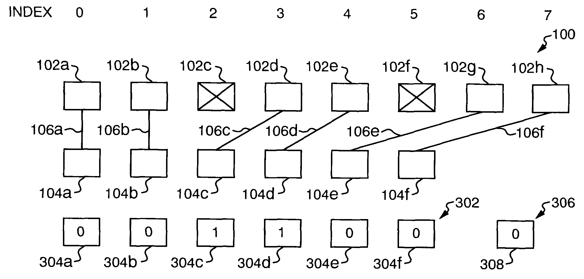
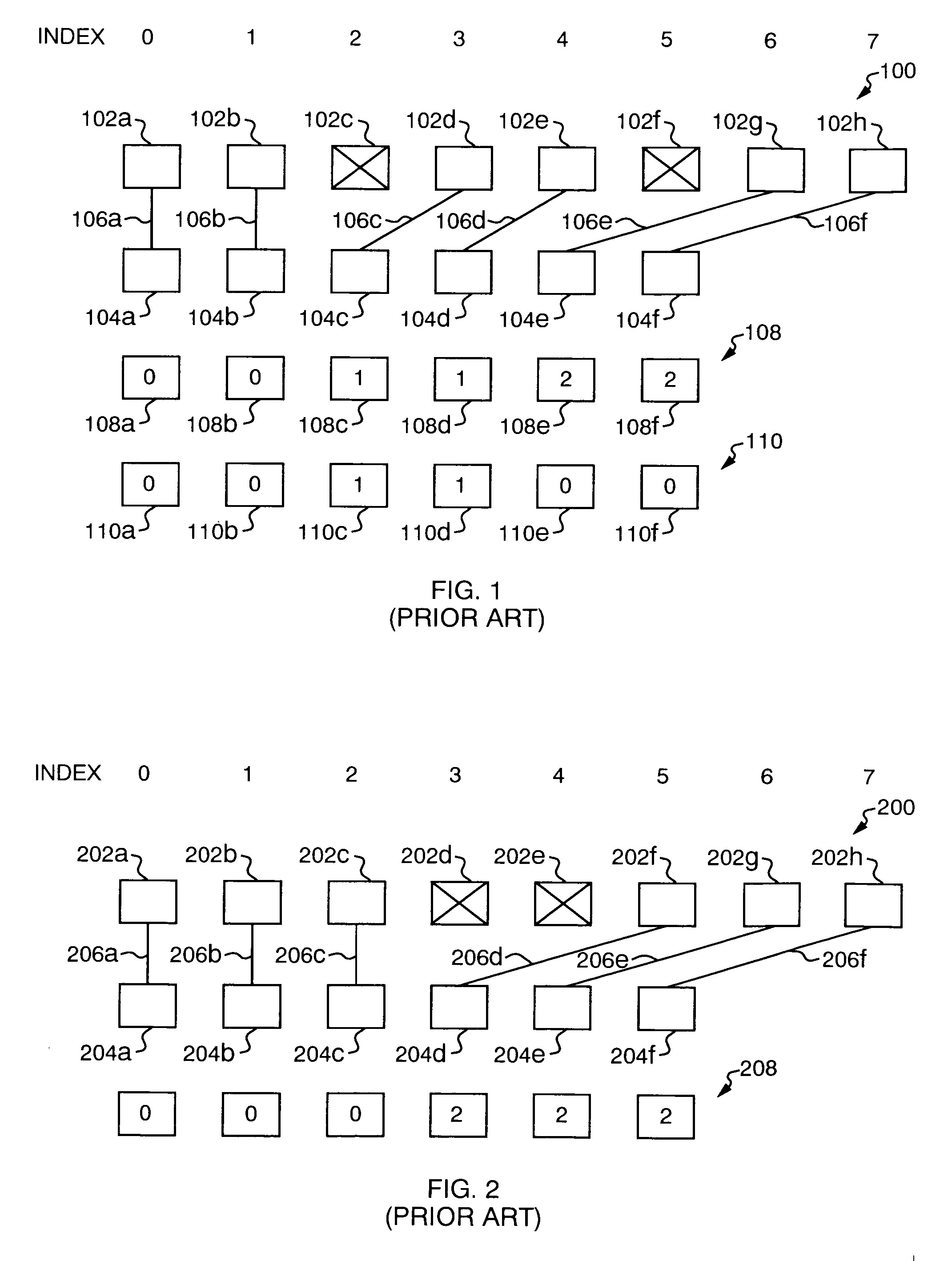
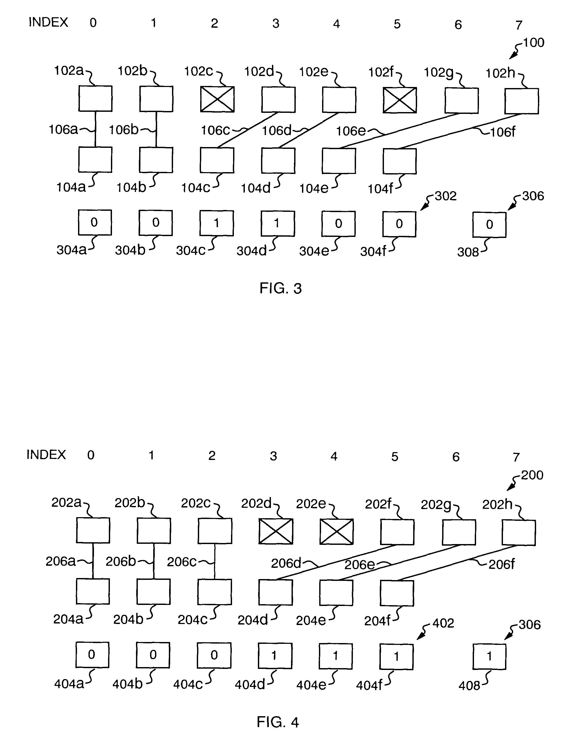
Techniques are disclosed for encoding mappings between functional (i.e., non-defective) bits in a digital memory and input / output ports for accessing the functional bits. Such mappings may be encoded in a shift encoding that includes a shift redundancy pattern and a hints table. The shift redundancy pattern may indicate positions of transitions from functional bits to defective bits in the digital memory. The hints table may indicate the number of defective bits in each set of consecutive defective bits in the digital memory. The combination of the shift redundancy pattern and hints table may be used to electrically connect the memory input / output ports to corresponding functional bits in the digital memory, thereby bypassing the defective bits and effectively repairing the memory. The shift encoding may be stored using a relatively small number of circuit elements and accessed relatively quickly to perform memory repair.

Before describing embodiments of the present invention in m...


PUM


Abstract

A computer system is disclosed that includes a memory, a memory defect map, and a shift encoder. The memory includes a plurality of bits and a plurality of input/output ports for accessing the plurality of bits. The memory defect map specifies positions of defective ones of the plurality of bits. The shift encoder encodes positions of defective ones of the plurality of bits in a shift encoding. The shift encoding includes a shift redundancy record representing positions of transitions between functional bits and defective bits in the memory, and a hints record representing numbers of bits in sets of consecutive defective bits in the memory.

Description

BACKGROUND Integrated circuits are becoming increasingly small and densely packed. It is now possible, for example, to manufacture individual digital memory cells having an area of less than one square micron, and to pack hundreds of millions of transistors on a memory chip that is smaller than a dime. Due to uncontrollable variations in the manufacturing process, it is not possible to manufacture such memory chips perfectly. Any particular memory chip may include any number and variety of defects. For example, one or more memory cells on a chip may be defective and therefore be unable to store data reliably. For a memory chip to be usable, however, the chip must be functionally indistinguishable from a chip having no defects. Because it is not possible to manufacture an actual defect-free chip, various techniques have been developed for automatically repairing defective chips so that they can provide the same functionality as a defect-free chip. Although it may not be possible to...

Claims


Application Information

Patent Timeline
Patent Type & Authority Applications(United States)
IPC IPC(8): G06F11/00
CPCG11C29/4401G11C29/848G11C29/802
Inventor WUU, JOHN J.WEISS, DONALD R.UNANGST, MATTHEW RYAN
Owner HEWLETT PACKARD DEV CO LP
Why Eureka
Try Eureka