Method of driving plasma display panel

a plasma display panel and plasma technology, applied in the field of plasma display panel driving, can solve the problems of complex driving circuit, inferior display quality of interlace mode, and long addressing technique, and achieve the effect of sufficient driving margin and easy production

Inactive Publication Date: 2005-03-10
FUJITSU HITACHI PLASMA DISPLAY LTD
View PDF5 Cites 15 Cited by
  • Summary
  • Abstract
  • Description
  • Claims
  • Application Information

AI Technical Summary

Benefits of technology

[0011] Thus, the present invention provides a method of driving a plasma display panel having a plurality of display electrodes and a plurality of address electrodes arranged orthogonally to each other between a pair of substrates forming a discharge space, display lines being defined between adjacent display electrodes by surface discharge, cells being defined at positions of intersection of the display lines and the address electrodes, a single display electrode between two adjacent display lines being utilized as a scan electrode at the time of producing address discharge to select a cell to illuminate, the method comprising: controlling a charge state of a first display line being one of the two adjacent display lines utilizing the same single scan electrode, such that address discharge is not generated and controlling a charge state of a second display line being the other of the two adjacent display lines, such that address discharge can be generated, an

Problems solved by technology

However, the interlace mode is inferior in display quality to a so-called progressive mode in which the display lines are scanned in sequence.
However, the technique take

Method used


Image

  • Method of driving plasma display panel
  • Method of driving plasma display panel
  • Method of driving plasma display panel

Examples


first embodiment

[0055]FIG. 5 illustrates waveforms of applied voltages according to the method of driving the PDP.

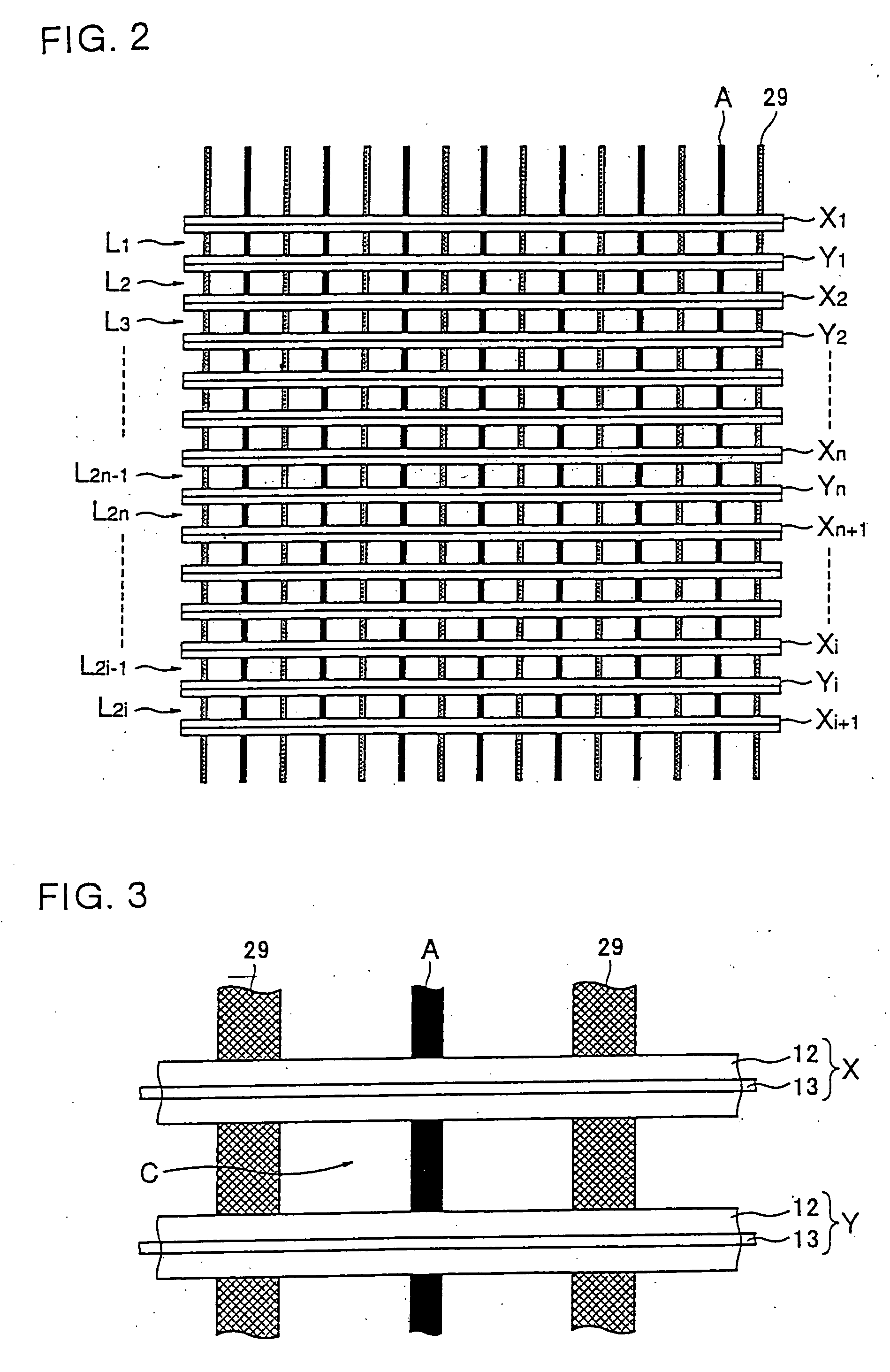
[0056] In the ALiS type PDP, Y electrodes to be used as scan electrodes and X electrodes to which the scan pulse is not applied are alternately arranged. The Y electrodes can independently be controlled because the scan pulse is applied thereto. Among the X electrodes, odd-numbered X electrodes are classified as a first group (Xodd electrodes) and even-numbered X electrodes are classified as a second group (Xeven electrodes). The Xodd electrodes and the Xeven electrodes are commonly connected, respectively.

[0057] During the first half of the address period, display lines between the Xodd electrodes and the Y electrodes are addressed. During the second half of the address period display lines between the Xeven electrodes and the Y electrodes are addressed. Thereafter, discharge is taken place in all the display lines simultaneously.

[0058] Specifically, the reset period TR is divided in...

second embodiment

[0125] In the above explanation of the second embodiment the second reset period TR12 of the odd-numbered subframe is described to have two sequences of the first step TR12a and the second step TR12b. In further detail the second step TR12b is divided into two sequences of Write and Charge adjustment. Accordingly, hereinafter the second reset period TR12 of the odd-numbered subframe is consisted of the first step TR12a, the second step TR12b and the third step TR12c.

[0126] The second reset period TR22 of the even-numbered subframe is also described to have two sequences of the first step TR22a and the second step TR22b, but in further detail, the second step TR22b is consisted of two sequences of Write and Charge adjustment. Hereinafter the second reset period TR22 of the even-numbered subframe is consisted of the first step TR22a, the second step TR22b and the third step of TR22c.

[0127] Each of the subframes has the same sequence as that of the first embodiment except that the fi...

fourth embodiment

[0146]FIG. 13 illustrates waveforms of applied voltages of the method of driving the PDP according to the present invention.

[0147] The fourth embodiment is a variation of the second embodiment. The initialization in the first half is simplified in the second embodiment, whereas the initialization in the second half is also simplified in the fourth embodiment. If the initialization in the second half is simplified, cells that were not discharged in the preceding subframe are not driven but those discharged in the preceding subframe can be driven.

[0148] The first half of the fourth embodiment is the same as that of the second embodiment. In the second half, only the charge adjustment is carried out in the second step TR2b in the second reset period. That is, according to the charge adjustment, wall voltage generated between the A electrodes and the Y electrodes are adjusted to be not less than a value obtained by reducing a voltage applied between the A and Y electrodes at the addres...


PUM


Abstract

A method of driving a plasma display panel, which includes controlling a charge state of a first display line being one of the two adjacent display lines utilizing the same single scan electrode, such that address discharge is not generated and controlling a charge state of a second display line being the other of the two adjacent display lines, such that address discharge can be generated, and then generating address discharge in the second display line, controlling the charge state of the second display line such that address discharge is not generated and controlling the charge state of the first display line such that the address discharge can be generated, and then generating address discharge in the first display line, and generating surface discharge simultaneously in the first and second display lines, thereby to achieve progressive display.

Description

CROSS-REFERENCE TO RELATED APPLICATION [0001] This application is a continuation of application Ser. No. 09 / 986,922, filed Nov. 13, 2001, now pending. Further, this application is related to Japanese application No. 2001-185387 filed on Jun. 19, 2001, whose priority is claimed under 35 USC §119, the disclosure of which is incorporated by reference in its entirety.BACKGROUND OF THE INVENTION [0002] 1. Field of the Invention [0003] The present invention relates to a method of driving a plasma display panel (PDP) and more particular to a method of driving a plasma display panel comprising a plurality of display electrodes for producing surface discharge and a plurality of address electrodes (signal electrodes) for selection arranged orthogonally to each other between a pair of substrates. [0004] 2. Description of Related Art [0005] In the above-described PDP, the display electrodes are extended in a row direction of a screen and arranged parallel to each other to have equal spaces ther...

Claims


Application Information

Patent Timeline
IPC IPC(8): H04N5/66G09G3/20G09G3/288G09G3/291G09G3/292G09G3/293G09G3/294G09G3/298G09G3/299
CPCG09G3/2927G09G3/2932G09G3/2935G09G2310/066G09G3/299G09G2310/0205G09G3/294G09G3/293
Inventor SHIIZAKI, TAKASHIHIRAKAWA, HITOSHI
Owner FUJITSU HITACHI PLASMA DISPLAY LTD
Why Eureka
Try Eureka