Method for making a microstructure by surface micromachining

a microstructure and surface micromachining technology, applied in the manufacture of microstructure devices, microstructure technology, microstructure devices, etc., can solve the problems of obvious detrimental effect of microstructure on optical performance capabilities, and achieve the effect of enhancing the distribution of etchants and enhancing the release of simple, single structural layers

Inactive Publication Date: 2005-03-17
MEMX
View PDF22 Cites 60 Cited by
  • Summary
  • Abstract
  • Description
  • Claims
  • Application Information

AI Technical Summary

Benefits of technology

[0006] Various refinements exist of the features noted in relation to the first aspect of the present invention. Further features may also be incorporated in the first aspect of the present invention as well. These refinements and additional features may exist individually or in any combination. In one embodiment, at least one end of at least one etch release conduit may be disposed at least generally at the same radial position as a perimeter of the first structural layer. Hereafter, “at least generally at the same radial position” in relation to any end of any etch release conduit or structure used to define the same means within 50 μm of the radial position of the perimeter of the relevant structural layer in one embodiment, more preferably within 25 μm of the radial position of the perimeter of the relevant structural layer in another embodiment, and even more preferably at the same radial position as the perimeter of the relevant structural layer. As such, the etchant does not have to etch in from the perimeter “too far” before encountering an open end of one or more etch release conduits associated with the first aspect. Reducing the time required for the etchant to reach the etch release conduits should at least to a point reduce the overall time for accomplishing the release of the microstructure from the substrate.
[0025] Various refinements exist of the features noted in relation to the third aspect of the present invention. Further features may also be incorporated in the third aspect of the present invention as well. These refinements and additional features may exist individually or in any combination. The higher etch rate in the low density regions of the first sacrificial layer may define a plurality of at least generally laterally extending etch release pipes, channels, conduits, or the like, which in turn should reduce the time required to completely release the microstructure from the first substrate. Although the low density regions will typically be disposed at a constant elevation relative to the substrate, such need not be the case.
[0029] One advantage of the above-noted method for defining the low density regions in accordance with the third aspect, and thereby for defining a plurality of etch release channels, is that a layout of the low density regions may define a network or grid-like structure or such that a plurality of these low density regions cross and / or are interconnected in some manner. For instance, the patterning of the second sacrificial layer could define a repeating pattern of interconnected “diamonds,” a honeycomb or honeycomb-like structure, or the like. This ability to define a network could further enhance the distribution of the etchant during the release of the first structural layer from the first substrate. Another advantage of this particular method for defining the low density regions, and thereby for defining a plurality of etch release channels, is that the same does not require the use of any structural layer or material for the formation thereof. Therefore, this particular embodiment of the third aspect could be used to enhance the release of a simple, single structural layer in a microstructure.

Problems solved by technology

The presence of these small holes on the upper surface of the mirror microstructure has an obvious detrimental effect on its optical performance capabilities.

Method used


Image

  • Method for making a microstructure by surface micromachining
  • Method for making a microstructure by surface micromachining
  • Method for making a microstructure by surface micromachining

Examples


Embodiment Construction

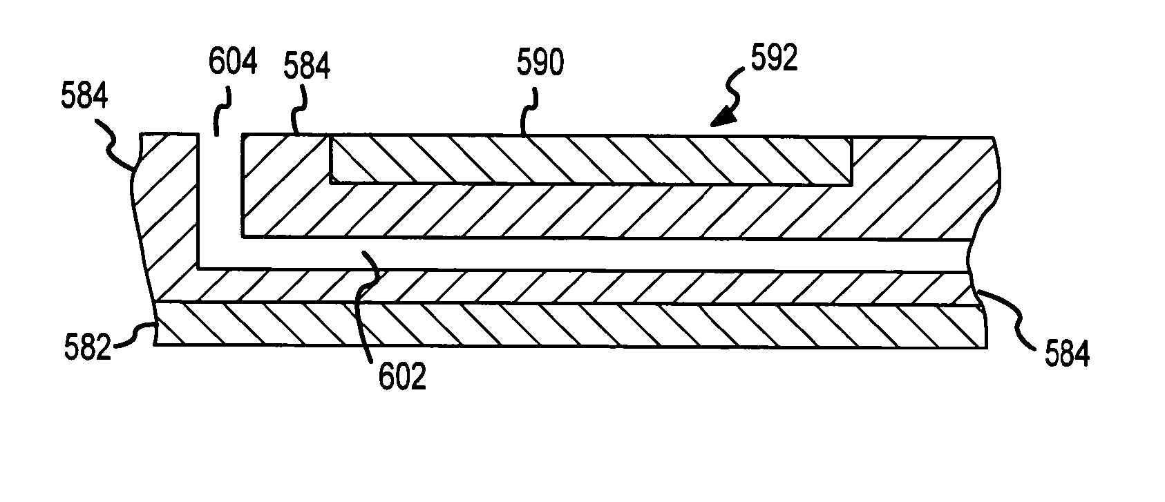
[0068] The present invention will now be described in relation to the accompanying drawings which at least assist in illustrating its various pertinent features. Surface micromachined microstructures and methods of making the same are the general focus of the present invention. Various surface micromachined microstructures and surface micromachining techniques are disclosed in U.S. Pat. Nos. 5,783,340, issued Jul. 21, 1998, and entitled “METHOD FOR PHOTOLITHOGRAPHIC DEFINITION OF RECESSED FEATURES ON A SEMICONDUCTOR WAFER UTILIZING AUTO-FOCUSING ALIGNMENT”; U.S. Pat. No. 5,798,283, issued Aug. 25, 1998, and entitled “METHOD FOR INTEGRATING MICROELECTROMECHANICAL DEVICES WITH ELECTRONIC CIRCUITRY; U.S. Pat. No. 5,804,084, issued Sep. 8, 1998, and entitled “USE OF CHEMICAL MECHANICAL POLISHING IN MICROMACHINING”; U.S. Pat. No. 5,867,302, issued Feb. 2, 1999, and entitled “BISTABLE MICROELECTROMECHANICAL ACTUATOR”; and U.S. Pat. No. 6,082,208, issued Jul. 4, 2000, and entitled “METHOD ...


PUM


Abstract

Various methods for forming surface micromachined microstructures are disclosed. One aspect relates to executing surface micromachining operation to structurally reinforce at least one structural layer in a microstructure. Another aspect relates to executing the surface micromachining operation to form a plurality of at least generally laterally extending etch release channels within a sacrificial material to facilitate the release of the corresponding microstructure.

Description

FIELD OF THE INVENTION [0001] The present invention generally relates to making a microstructure by surface micromachining. One aspect relates to making a structurally reinforced microstructure to provide a flatter profile on one or more of its structural layers. Another aspect relates to providing a plurality of at least generally laterally extending etch release channels to facilitate the release of the microstructure from the substrate. BACKGROUND OF THE INVENTION [0002] There are a number of microfabrication technologies that have been utilized for making microstructures (e.g., micromechanical devices, microelectromechanical devices) by what may be characterized as micromachining, including LIGA (Lithographie, Galvonoformung, Abformung), SLIGA (sacrificial LIGA), bulk micromachining, surface micromachining, micro electrodischarge machining (EDM), laser micromachining, 3-D stereolithography, and other techniques. Bulk micromachining has been utilized for making relatively simple ...

Claims


Application Information

Patent Timeline
Patent Type & Authority Applications(United States)
IPC IPC(8): H01L21/00H01L21/302H01L21/304H01L21/461
CPCB81C1/00547H01L21/302
Inventor SNIEGOWSKI, JEFFRY J.RODGERS, M. STEVEN
Owner MEMX
Why Eureka
Try Eureka