
Hole transport material and method of manufacturing the hole transport material

a technology of transport material and hole, which is applied in the direction of discharge tube luminescnet screen, non-metal conductor, conductor, etc., can solve the problems of specific index, light-emission luminance, light-emission luminance reduction or deterioration, etc., and achieve the effect of suppressing the decrease of light-emission luminan

Inactive Publication Date: 2005-03-24
SEIKO EPSON CORP
View PDF16 Cites 16 Cited by
  • Summary
  • Abstract
  • Description
  • Claims
  • Application Information

AI Technical Summary

Benefits of technology

It is therefore an object of the present invention to provide a hole transport material which can suppress the decrease of light-emission luminance in an organic EL device, and a method of manufacturing the hole transport material.
According to the manufacturing methods of the present invention described above, it is possible to eliminate anionic impurities and / or cationic impurities from a hole transport material with relatively ease and in a relatively short period of time. Further, according to the invention, only by appropriately selecting the kind of eliminating means to be used, it is possible to eliminate target anionic impurities and / or cationic impurities reliably and efficiently.

Problems solved by technology

However, from the viewpoint of practical use, the existing organic EL devices still have a problem in that light-emission luminance thereof is decreased or deteriorated when it is used over a long period of time, and therefore there is a demand for the establishment of technical measures to solve the problem.
However, specific indexes of the relationship between the decrease of light-emission luminance in an organic EL device and the kinds of impurities contained in the constituent materials to be used and their amounts contained therein have not yet been established.

Method used


Image

  • Hole transport material and method of manufacturing the hole transport material

Examples


example 1

A 2.0 wt % aqueous soloution of poly(3,4-ethylenedioxythiophene / styrenesulfonic acid) solution (which is a hole transport material and is manufactured by Bayer Corp. under the product name of “Baytron P”) was prepared as a solution for refinement.

Next, this solution for refinement was passed through a column provided with six filters at a solution temperature of 20° C. and at a liquid passage rate of 50 mL / min, to eliminate anionic impurities.

In this regard, it is to be noted that all of the filters were made of a styrene-based quaternary ammonium salt-type strongest basic anion-exchange resin.

Next, a solvent in the solution for refinement that has been passed through the filters was volatilized to remove it, to thereby obtain a refined hole transport material.

example 2

Refinement of a hole transport material was carried out in the same manner as in Example 1 except that all of the six filters were replaced with filters made of a styrene-based ethanolamine (quaternary ammonium salt)-type strongly basic anion-exchange resin.

example 3

Refinement of a hole transport material was carried out in the same manner as in Example 1 except that all of the six filters were replaced with filters made of an acrylic quaternary ammonium salt-type medium basic anion-exchange resin.


PUM

PropertyMeasurementUnit
volume resistivityaaaaaaaaaa
thicknessaaaaaaaaaa
thicknessaaaaaaaaaa

Abstract

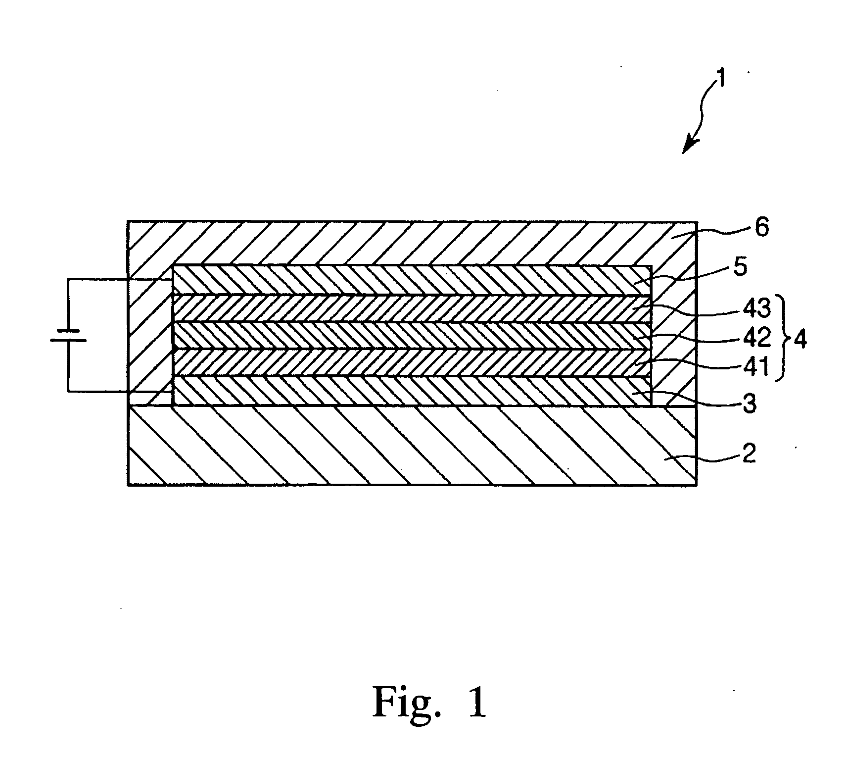
In an organic EL device, when a voltage is applied across an anode and a cathode, holes are moved in a hole transport layer and electrons are moved in an electron transport layer, and the holes and the electrons are recombined in a light emitting layer. In the light emitting layer, excitons are produced by energy released upon the recombination, and the excitons release energy in the form of fluorescence or phosphorescence or emit light when returning to the ground state. The hole transport material is used in the hole transport layer, in which the amount of cationic impurities and / or the amount of anionic impurities are controlled to be small, so that the decrease of light-emission luminance of the organic EL device is suppressed and excellent light emitting properties are maintained for a long period of time.

Description

BACKGROUND OF THE INVENTION 1. Field of the Invention The present invention relates to a hole transport material to be used for a layer having the function of transporting holes in an organic electroluminescent device (element), and a method of manufacturing the hole transport material. 2. Description of the Prior Art There is known an organic electroluminescent device (hereinafter, referred to as an “organic EL device”). The organic EL device has a structure in which at least one light emitting organic layer (organic electroluminescent layer) is provided between a cathode and an anode. Such an organic EL device can significantly reduce a voltage to be applied as compared with an inorganic EL device. Further, it is also possible to manufacture devices that can provide various luminescent colors. Currently, in order to obtain higher-performance organic EL devices, various researches are being actively carried out in developments and improvements of materials to be used as well a...

Claims


Application Information

Patent Timeline
Patent Type & Authority Applications(United States)
IPC IPC(8): C09K11/06H01L51/30H01L51/40H01L51/50
CPCH01L51/0003H01L51/5048H01L51/0037H10K71/12H10K85/1135H10K50/14C09K11/06Y10S428/917H10K50/15
Inventor SHINOHARA, YUJIISHII, RYUJISHIMAZU, MASAMITSUUEHARA, MASAMITSU
Owner SEIKO EPSON CORP
Learn More