Hole transport material, layer formed from the hole transport material, organic electroluminescent device, and method of manufacturing the hole transport material
a technology of transport material and transport layer, which is applied in the direction of discharge tube luminescent screen, conductor, non-metal conductor, etc., can solve the problems of specific index, light-emission luminance, and decreased or deteriorated light-emission luminance, so as to eliminate non-ionic impurities from the hole transport material reliably and efficiently, and the effect of short time period
- Summary
- Abstract
- Description
- Claims
- Application Information
AI Technical Summary
Benefits of technology
Problems solved by technology
Method used
Image
Examples
first embodiment
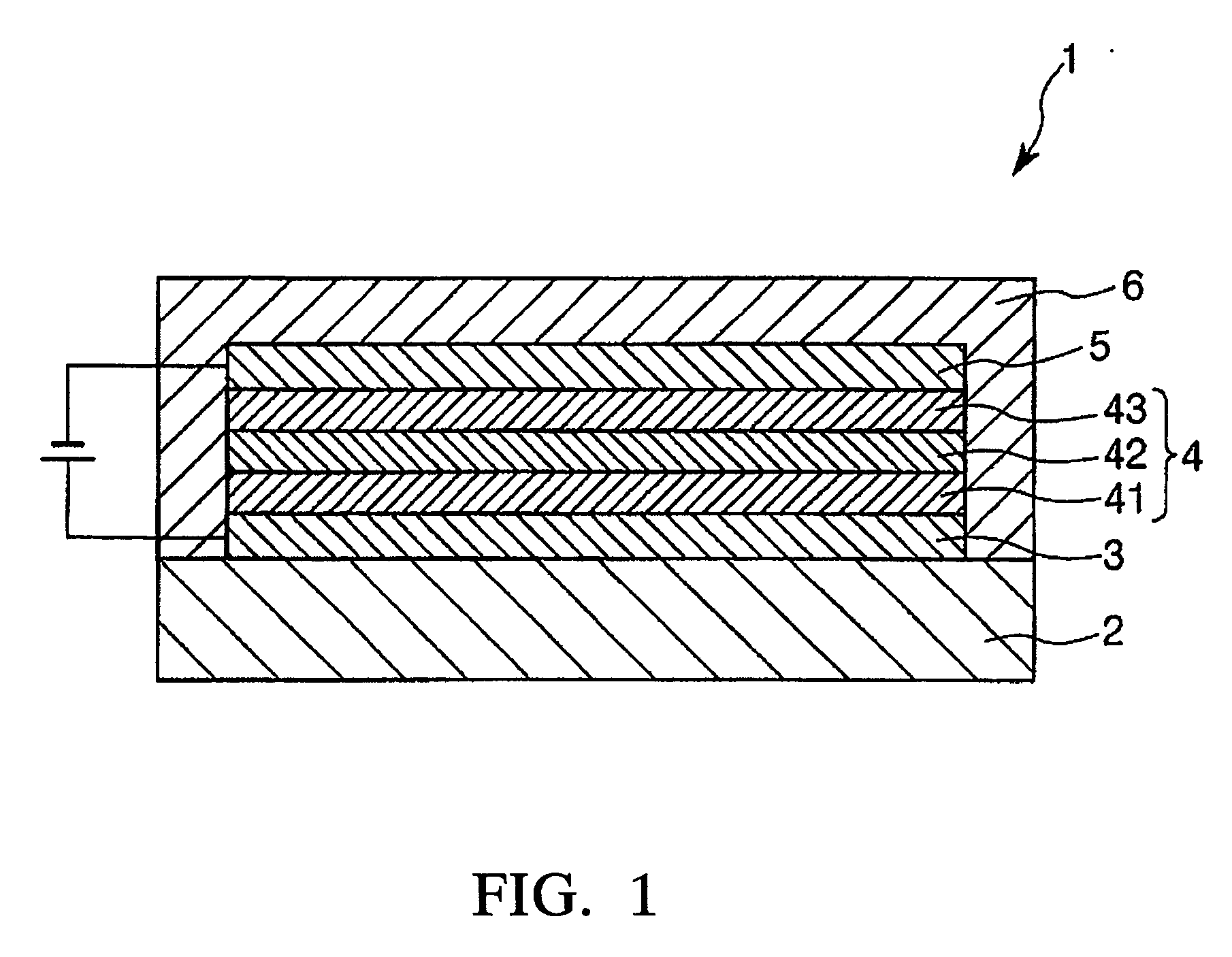
[0121] In order to suppress the decrease of light-emission luminance of the organic EL device, the present inventors have made extensive researches and studies for all the layers constituting the organic EL device, and in particular they have paid their attentions to a layer having the function of transporting holes.
[0122] As a result, the present inventors have found that the decrease of light-emission luminance of the organic EL device can be effectively suppressed by controlling an amount of impurities contained in the layer having the function of transporting holes, especially the amount of nonionic impurities having a molecular weight of 5,000 or less (hereinafter, simply referred to as “nonionic impurities”) to within a predetermined amount, leading to the completion of the present invention. In the specification, this will be described as a first embodiment.
[0123] As described above, there are known a hole injection layer and the like besides a hole transport layer as a lay...
second embodiment
[0155] In addition to the above, the present inventors have also found that the decrease of light-emission luminance of the organic EL device can be effectively suppressed by controlling amounts of anionic impurities, cationic impurities and nonionic impurities having a molecular weight of 5,000 or less (hereinafter, simply referred to as “nonionic impurities”) to within predetermined amounts, respectively, leading to the completion of the present invention. In the specification, this will be described as a second embodiment.
[0156] If the amounts of impurities such as nonionic impurities, anionic impurities and cationic impurities contained in the hole transport layer are large, a reaction between the hole transport material and the impurities occurs, or a structural change (decomposition and the like, for example) of the hole transport material occurs due to the impurities acting as a trigger, resulting in the deterioration of the hole transport layer with the elapse of time. Furt...
examples of first embodiment
[0209] First, a description will be made with regard to examples of the first embodiment directed to an amount of nonionic impurities having a molecular weight of 5,000 or less contained in a hole transport material and a hole transport layer.
[0210] In this regard, it is to be noted that no nonionic impurities were detected in the ultrapure water used in each of Examples and Comparative Examples described below.
[0211] Further, five organic EL devices were manufactured in each of Examples and Comparative Examples described below.
1. Method for Manufacturing Organic EL Device
PUM
| Property | Measurement | Unit |
|---|---|---|
| Fraction | aaaaa | aaaaa |
| Fraction | aaaaa | aaaaa |
| Fraction | aaaaa | aaaaa |
Abstract
Description
Claims
Application Information
