Liquid crystal display panel having dummy column spacer with opened portion

a liquid crystal display and spacer technology, applied in non-linear optics, instruments, optics, etc., can solve the problems of contaminating the liquid crystal, affecting the quality of liquid crystal display, so as to prevent imperfect or excessive filling and prevent imperfect filling

Inactive Publication Date: 2005-03-24
LG DISPLAY CO LTD
View PDF49 Cites 11 Cited by
  • Summary
  • Abstract
  • Description
  • Claims
  • Application Information

AI Technical Summary

Benefits of technology

[0020] Another object of the present invention is to provide a liquid crystal display panel and a method for fabricating the same to have a uniform cell gap and improved picture characteristics.
[0026] Accordingly, the present invention suggests dropping more than an amount of liquid crystal measured according to a cell gap and a substrate size for preventing imperfect filling, and forming a dummy column spacer in the dummy region to regulate a liquid crystal flow, for preventing imperfect or excessive filling of the liquid crystal.
[0027] Moreover, the regulation of the liquid crystal flow by the dummy column spacer solves the problem of the contamination of the liquid crystal by the contact with the UV sealant.

Problems solved by technology

However, the vacuum injection method takes much time to fill the liquid crystal between the substrates.
As a result, productivity is much reduced as the substrate becomes large.
Accordingly, if a thermo-hardening sealant is used to bond the substrates, it may flow and contaminate the liquid crystal during the heating process.
However, the related art liquid crystal dropping method has the following disadvantages caused by difficulty in determining an accurate amount of the liquid crystal depending upon a size of the substrate and a cell gap between the substrates.
First, if a dropped amount of the liquid crystal is less than the required amount, regions of the substrate for the liquid crystal are filled imperfectly.
Second, if the liquid crystal is dropped excessively, the liquid crystal comes into contact with the sealant before the sealant is hardened.
Thus, the liquid crystal is contaminated.
Third, even if the liquid crystal is dropped appropriately, it takes time to spread the liquid crystal from the center part of the substrate to the corners, the farthest spots.
Accordingly, if the imperfectly filled region occurs as the liquid crystal is not spread to the corner-regions, a final inspection cannot be carried out.

Method used


Image

  • Liquid crystal display panel having dummy column spacer with opened portion
  • Liquid crystal display panel having dummy column spacer with opened portion
  • Liquid crystal display panel having dummy column spacer with opened portion

Examples


first embodiment

[0046]FIG. 3 illustrates a plane view of an LCD panel in accordance with the present invention.

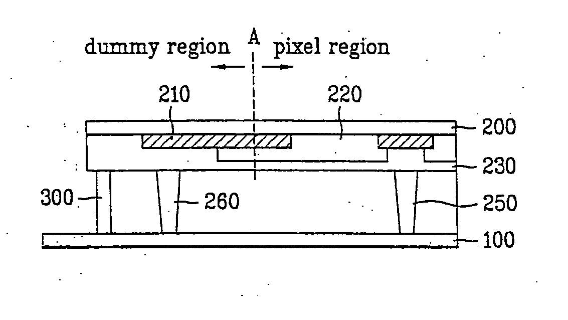
[0047] Referring to FIG. 3, the LCD panel includes a lower substrate 100, an upper substrate 200, and a UV sealant 300 between the substrates 100 and 200. Column spacers (not shown) are formed in a pixel region (a line ‘A’ represents an imaginary line for indicating a pixel region), and a dummy column spacer 260 is formed inside the UV sealant 300 in the dummy region to regulate a liquid crystal flow. A liquid crystal layer (not shown) is formed between the lower and upper substrates 100 and 200. The column spacer serves to maintain a cell gap between the lower substrate 100 and the upper substrate 200.

[0048] More specifically, the dummy column spacer 260 has a height the same as the column spacer, and an opened portion 262 in at least one of the corner-regions. Although the drawing shows that the opened portion 262 is formed at all four corners, the number of the opened portion 262 may b...

second embodiment

[0055]FIG. 5 illustrates a plane view of an LCD panel in accordance with the present invention.

[0056] Referring to FIG. 5, the LCD panel according to the second embodiment of the present invention includes a dummy column spacer 260 having an opened portion 262. The opened portion 262 includes a plurality of openings in each corner-region of the substrate.

[0057] The opened portion 262 including a plurality of openings permits a liquid crystal to easily flow to the corners of the substrate, and allows a uniform filling of the liquid crystal. The opened portion 262 may be formed in at least one of the corner-regions. A plurality of openings may be formed at either a constant interval or an irregular interval. The others are similar to the first embodiment.

third embodiment

[0058]FIG. 6 illustrates a plane view of an LCD panel in accordance with the present invention.

[0059] Referring to FIG. 6, the LCD panel includes a lower substrate 100, an upper substrate 200, and a UV sealant 300 between the lower and upper substrates 100 and 200. A plurality of column spacers (not shown) are formed in a pixel region (a line ‘A’ represents an imaginary line for indicating the pixel region), and a dummy column spacer 260 is formed on inside the UV sealant 300 in the dummy region to regulate a liquid crystal flow. The dummy column spacer 260 is formed at a height the same as the column spacer and has an opened portion 262 in at least one of the corner-regions. The opened portion 262 may not be formed at all. Also, a dotted line type dummy column spacer 270 may be additionally formed at the inner dummy region of the dummy column spacer 260 for assisting the regulation of the liquid crystal flow. A liquid crystal layer (not shown) is formed between the substrates 100 a...


PUM

PropertyMeasurementUnit
timeaaaaaaaaaa
thicknessaaaaaaaaaa
pressureaaaaaaaaaa

Abstract

A liquid crystal display panel and method for fabricating the same are disclosed in the present invention. The liquid crystal display panel includes first and second substrates facing into each other, a column spacer in a pixel region between the substrates, a dummy column spacer formed in a dummy region between the substrates, the dummy column spacer having an opened portion in at least one of corner-regions, a UV sealant formed outside the dummy column spacer between the substrates, and a liquid crystal layer between the substrates.

Description

[0001] This application claims the benefit of the Korean Application Nos. P2001-75459 filed on Nov. 30, 2001, P2001-79429 filed on Dec. 14, 2001, and P2002-18460 filed on Apr. 4, 2002, which are hereby incorporated by reference. BACKGROUND OF THE INVENTION [0002] 1. Field of the Invention [0003] The present invention relates to a liquid crystal display, and more particularly, to a liquid crystal display panel and method for fabricating the same by a liquid crystal dropping method. [0004] 2. Discussion of the Related Art [0005] A thin flat panel display tends to have a thickness of no more than a few centimeters. Particularly, a liquid crystal display (LCD) has a wide scope of applications, such as notebook computers, computer monitors, gauge monitors for space crafts, and air crafts, and the like. [0006] Referring to FIG. 1, an LCD is provided with a lower substrate 1 having a plurality of thin film transistors and pixel electrodes formed thereon, an upper substrate 3 facing into th...

Claims


Application Information

Patent Timeline
Patent Type & Authority Applications(United States)
IPC IPC(8): G02F1/1339G02F1/1341
CPCG02F1/1339G02F2001/13415G02F1/1341G02F1/13394G02F1/13415
Inventor KIM, JONG WOOKANG, SUNG CHUNHA, YOUNG HUN
Owner LG DISPLAY CO LTD
Why Eureka
Try Eureka