
Eureka
For R&D, Eureka makes reading and utilizing patents & technical documents easy.
Eureka AIR
Designed for self-driven R&D workflows. Generate viable solutions, solve complex R&D challenges, empower your innovation with AI.

Eureka Materials
Designed for material experts only. Revolutionize your material R&D, from search, analyze, to developing new materials.

TechResearch
Generate reliable direction feasibility study reports for your R&D in just a few steps.

TechSeek
Discover and master advanced knowledge NOW. Basics, ideas, possibilities, all at once.

TechMind
As an expert in R&D Theories, TechMind can generates customized viable solutions instantly.

TechRisk
Analyze your overall solution with one click, know your potential R&D risks in advance.

TechMonitor
Get weekly tech updates, stay abreast of the latest tech innovations and key insights.
Data read/write control system and data read/write control method
- Summary
- Abstract
- Description
- Claims
- Application Information
AI Technical Summary
Benefits of technology
Problems solved by technology
Method used
Image

Examples
embodiment 1
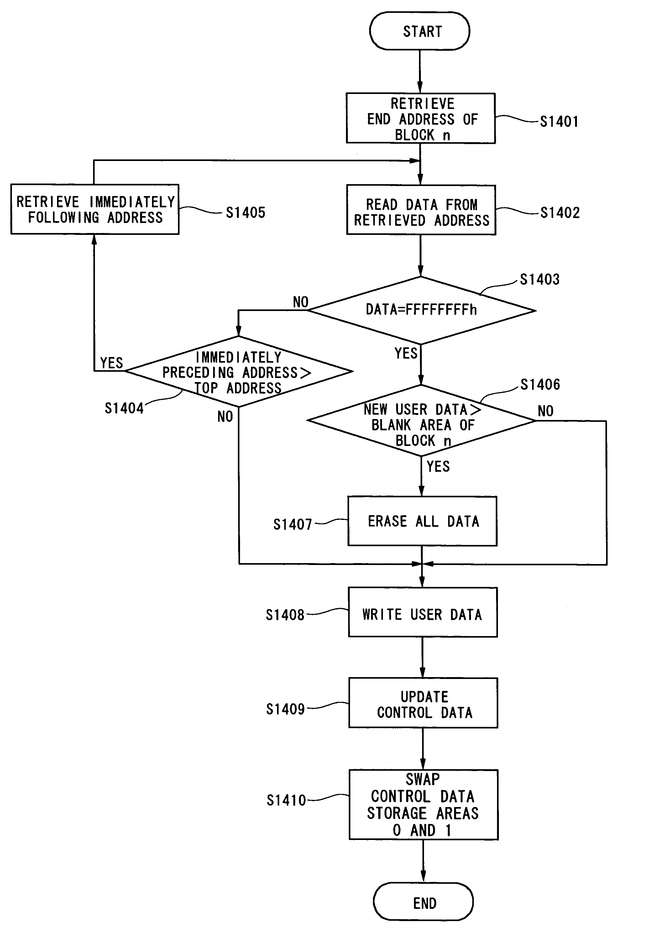
[0078] Embodiment 1
[0079] A first embodiment of the present invention is explained hereinafter. The first embodiment describes a method of writing new user data and the size of the new user data to flash memory. This method allows flash memory to be used like EEPROM.
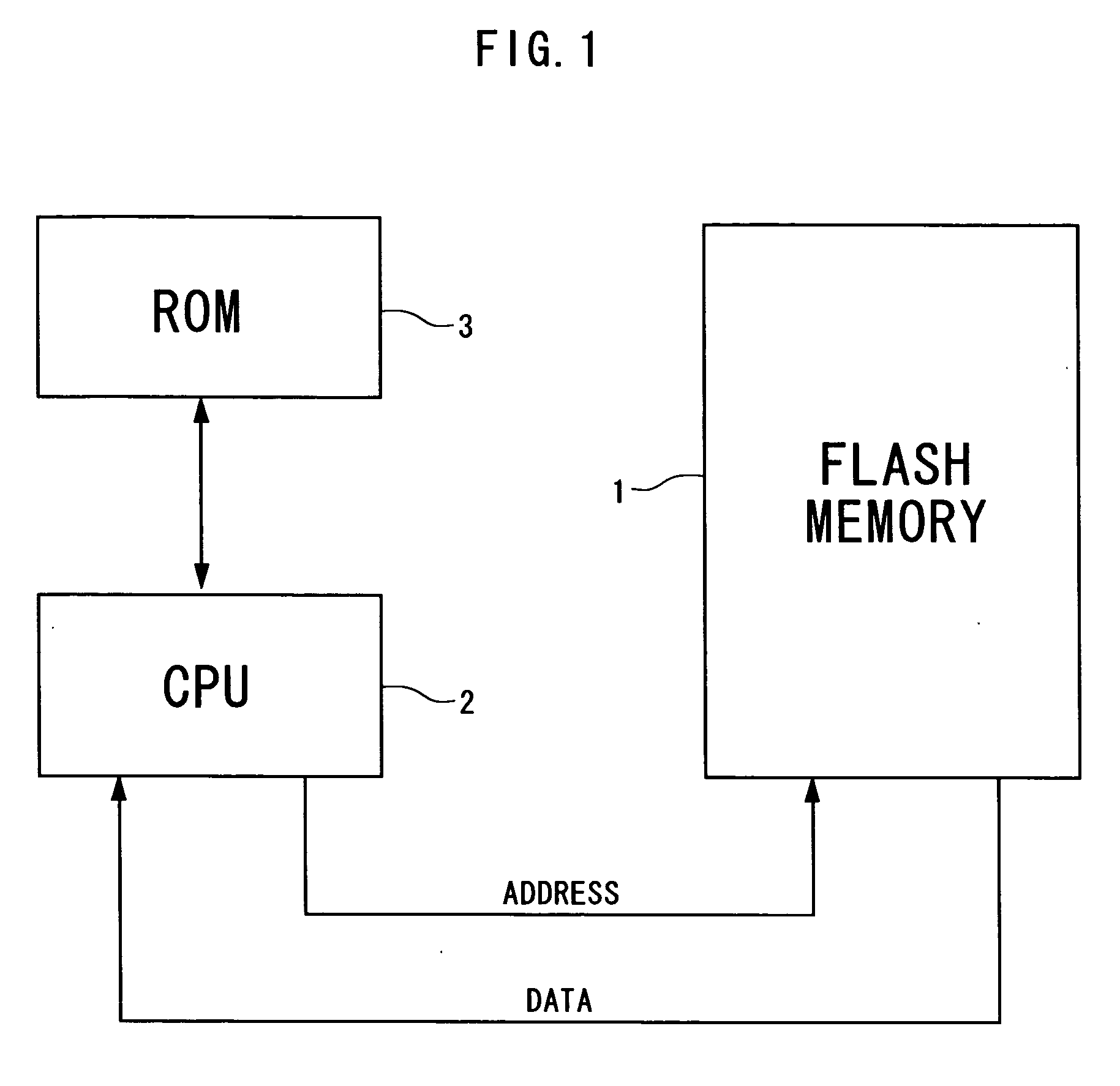
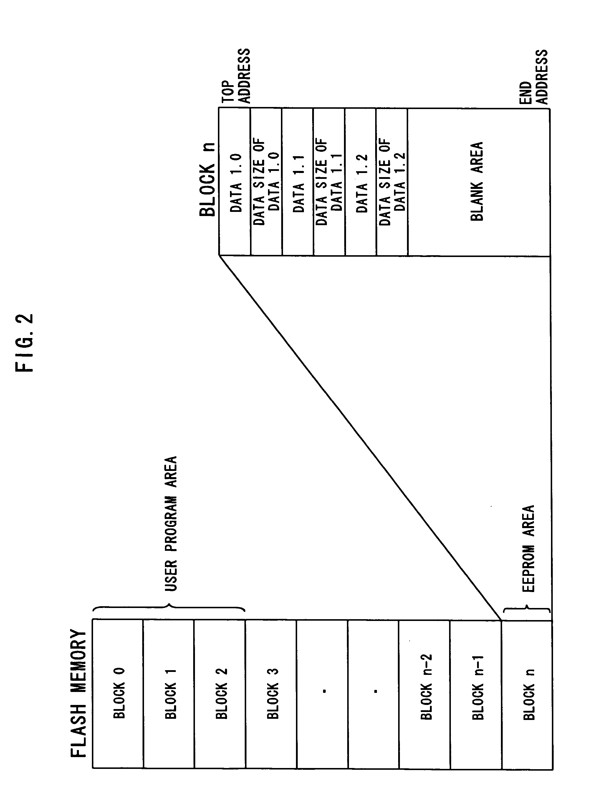
[0080]FIG. 1 shows the structure of the first embodiment. FIG. 2 shows the structure of flash memory.
[0081] Flash memory 1 shown in FIG. 1 is divided into a plurality of memory areas from Block 0 to n, as shown in FIG. 2. A user program area and an EEPROM area are predefined in Blocks 0 to n. The user program area stores various data. The EEPROM area is used as an alternative for EEPROM. This embodiment uses Block n as the EEPROM area.
[0082] A CPU 2 in FIG. 1 writes user data and the size of the user data to Block n, which is the EEPROM area of the flash memory 1. The user data and the user data size are sequentially written in this order from the top address of Block n. Though the CPU 2 writes four bytes of data each...
embodiment 2
[0103] Embodiment 2
[0104] A second embodiment of the present invention is explained hereinafter. Though the first embodiment describes the method of storing new user data and the size of the new user data sequentially from the top address of a block, the second embodiment describes the method of storing new user data and the size of the user data sequentially from the end address of a block.
[0105] The structure of the second embodiment is the same as that of the first embodiment shown in FIG. 1. FIG. 5 is a block diagram of the flash memory 1 according to the second embodiment.
[0106] The flash memory 1 is divided into a plurality of memory areas from Block 0 to n, as shown in FIG. 5. A user program area and an EEPROM area are predefined in Blocks 0 to n. The user program area stores various data. The EEPROM area is used as an alternative for EEPROM. The second embodiment also uses Block n as the EEPROM area.
[0107] The CPU 2 writes user data and the size of the user data to Block ...
embodiment 3
[0125] Embodiment 3
[0126] A third embodiment of the present invention is explained hereinafter. The structure of the third embodiment is the same as that of the first embodiment shown in FIG. 1. FIG. 8 is a block diagram of the flash memory 1 according to the third embodiment.
[0127] The flash memory 1 is divided into a plurality of memory areas from Block 0 to n, as shown in FIG. 8. A user program area and an EEPROM area are predefined in the Blocks 0 to n. The user program area stores various data. The EEPROM area is used as an alternative for EEPROM. The third embodiment also uses Block n as the EEPROM area.
[0128] The CPU 2 writes control data consisting of the size and pointer of new user data and user data sequentially in this order to Block n from the top address. The pointer is controlled by the type of data, which is, by the data of each application. The pointer of user data of each application is written with an address of the next user data. The pointer of the last user d...
PUM
 Abstract
Description
Claims
Application Information
 - R&D Engineer
- R&D Manager
- IP Professional
- Industry Leading Data Capabilities
- Powerful AI technology
- Patent DNA Extraction
Browse by: Latest US Patents, China's latest patents, Technical Efficacy Thesaurus, Application Domain, Technology Topic, Popular Technical Reports.
© 2024 PatSnap. All rights reserved.Legal|Privacy policy|Modern Slavery Act Transparency Statement|Sitemap|About US| Contact US: help@patsnap.com