Semiconductor radiological detector and semiconductor radiological imaging apparatus

a radiological detector and semiconductor technology, applied in the direction of radiation intensity measurement, instruments, x/gamma/cosmic radiation measurement, etc., can solve the problems of detector decline, sensitivity, spatial resolution, detector dead space, etc., to prevent the dead space of the signal line, improve detection sensitivity, and prevent the effect of signal line dead spa

Inactive Publication Date: 2005-03-31
HITACHI LTD
View PDF11 Cites 8 Cited by
  • Summary
  • Abstract
  • Description
  • Claims
  • Application Information

AI Technical Summary

Benefits of technology

[0005] It is an object of the present invention to provide a semiconductor radiological detector and a semiconductor radiological detecting apparatus which minimizes a dead space resulting from the draw-out of a signal line from an electrode and which allows semiconductor elements to be densely arranged to improve sensitivity and spatial resolution.
[0007] This configuration allows the signal lines to be extended straight from the electrode (anode or cathode) to prevent a dead space for the signal lines from being created around the semiconductor radiological detector.
[0008] The present invention enables the signal line to be extended straight along a surface of the electrode (anode or cathode) to prevent the dead space for the signal lines from being created around the semiconductor radiological detector. This enables a number of semiconductor radiological detectors to be densely arranged. Therefore, detection sensitivity is improved and nonuniformity at joints can be avoided.

Problems solved by technology

However, with the cross strip reading method, only 2×200 reading channels are required.
Thus, disadvantageously, the sensitivity, spatial resolution, and the like of the semiconductor radiological detector decrease, resulting in nonuniformity at joints.

Method used


Image

  • Semiconductor radiological detector and semiconductor radiological imaging apparatus
  • Semiconductor radiological detector and semiconductor radiological imaging apparatus
  • Semiconductor radiological detector and semiconductor radiological imaging apparatus

Examples


first embodiment

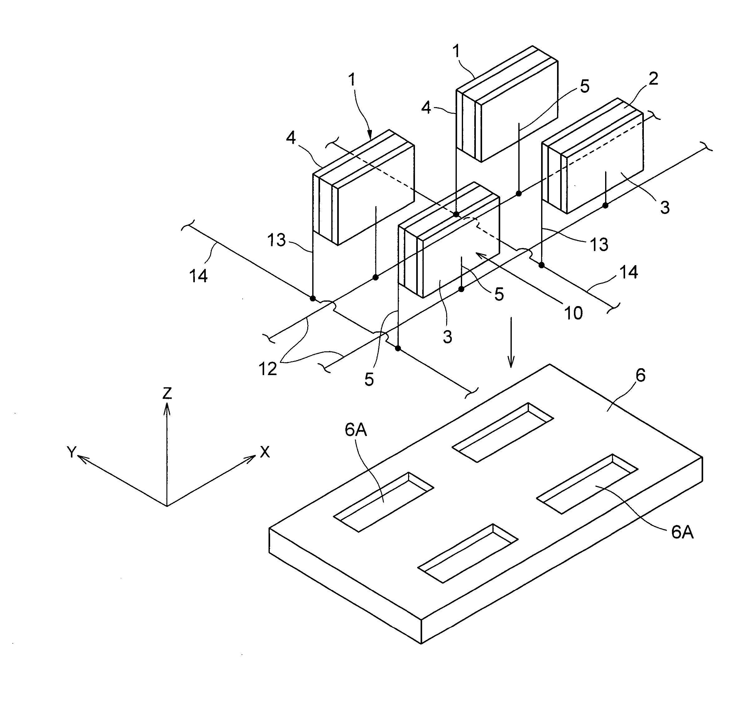
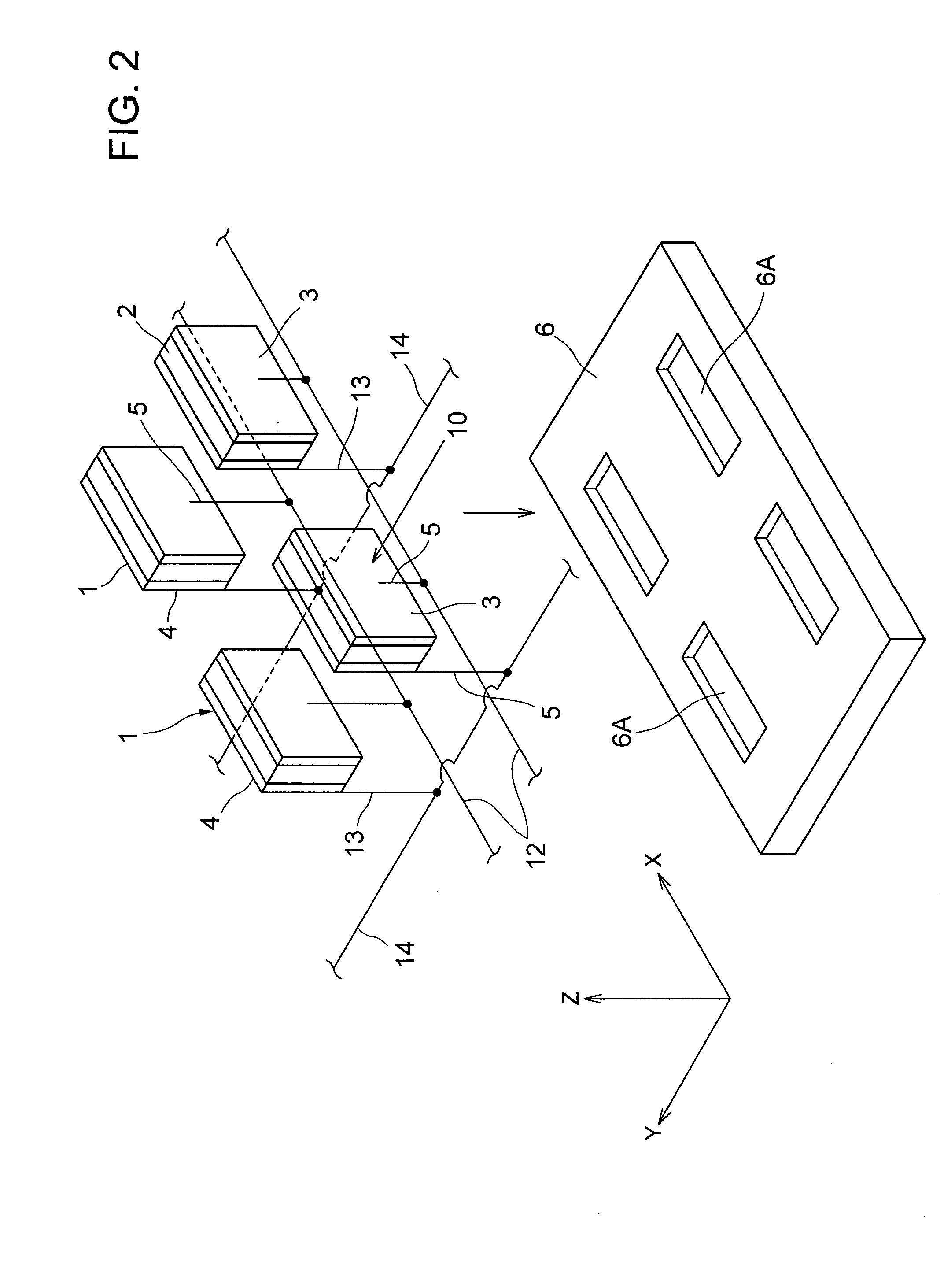
[0020] A first embodiment of the present invention will be described below with reference to FIGS. 1 and 2, which are accompanying drawings.

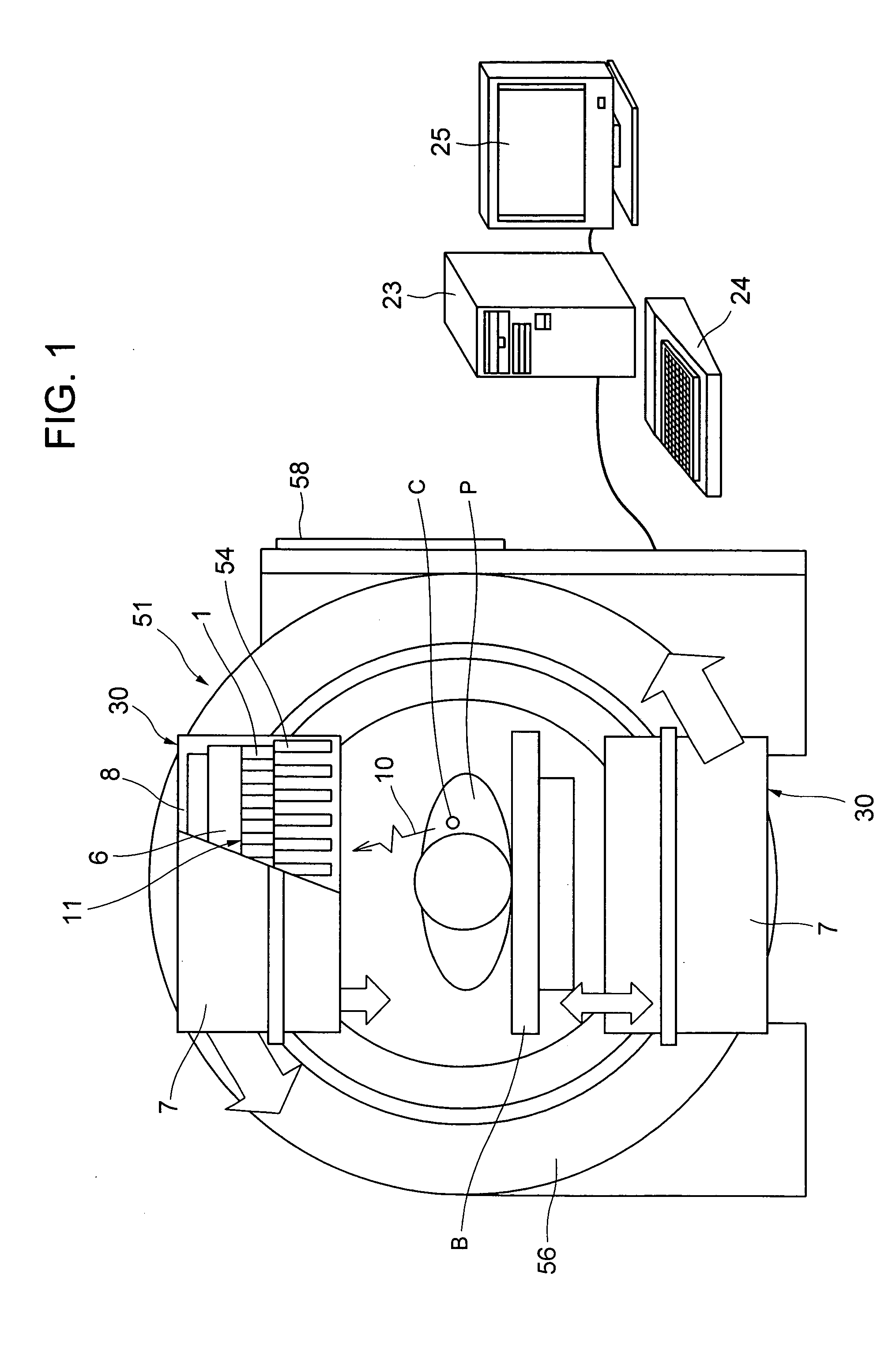
[0021] In FIG. 1, a SPECT (Single Photon Emission Computer Tomography) apparatus 51 that is a radiological imaging apparatus comprises paired semiconductor radiological detecting apparatuses 30, a rotating support table 56, a data collecting and analyzing apparatus 23, a data input apparatus 24, and a display apparatus 25. Paired semiconductor radiological detecting apparatuses 30 are arranged on the rotating support table 56 at an angle of 180° to each other in a circumferential direction. Specifically, socket board mounting substrates 6 of the semiconductor radiological detecting apparatuses 30 are mounted on the rotating support table 56 at an angle of 180° to each other in the circumferential direction. Each radiological detecting unit 11 faces a bed B. A collimator 54 is installed between the radiological detecting unit 11 and a patient P ...

second embodiment

[0031] Now, with reference to FIG. 3, description will be given of a second embodiment of the present invention.

[0032] In FIG. 3, a radiological detecting unit 60 comprises a plurality of semiconductor radiological detectors 61, 61, . . . (only four are shown) as in the case of the first embodiment. That is, if the thickness of a single semiconductor device 61 is simply increased, the distance between electrodes, in other words, a charge collection distance increases to reduce the energy resolution. However, in the present embodiment, a plurality of semiconductor radiological detectors 1 are arranged parallel to one another with the inter-electrode distance of a single device reduced. This provides a semiconductor radiological detector 1 having both high energy resolution and high detection efficiency. The semiconductor radiological detector 61 has two semiconductor devices 62, 62 arranged opposite each other, anodes 63, 63 placed between the semiconductor devices 62 and 62, and ca...

third embodiment

[0036] Now, a third embodiment of the present invention will be described with reference to FIGS. 4 and 7.

[0037] In FIG. 4, a radiological detecting unit 70 comprises a plurality of semiconductor radiological detectors 71, 71, . . . (only six of them are shown). The semiconductor radiological detector 71 is composed of two semiconductor devices 72A and 72B arranged opposite each other, anodes 73A and 73B placed between the semiconductor devices 72A and 72B, cathodes 74A and 74B placed opposite the anodes 73A and 73B via the semiconductor devices 72A and 72B, respectively, and a protective connector case 75 that accommodates the semiconductor devices 72A and 72B, the cathodes 73A and 73B, and the anodes 74A and 74B. A bottom part of the protective connector case 75 is provided with a cathode pin 76 that is a signal line connected to the cathodes 73A and 73B and an anode pin 77 that is another signal line connected to the anodes 74A and 74B. Further, a socket board 78 is formed with ...


PUM


Abstract

The semiconductor radiological detector 1 minimizes a dead space resulting from the draw-out of a signal line from an electrode and which allows a number of semiconductor devices to be densely arranged to improve sensitivity and spatial resolution. The semiconductor radiological detector 1 comprises a semiconductor device 2, an anode 3 attached to one surface of the semiconductor device 2, and a cathode 4 attached to the other surface of the semiconductor device 2. A signal line 5 is provided on the anode 3; the signal line 5 extends straight from the anode 3 and is connected to an X axis wire 12. Another signal line 13 is provided on the cathode 4; the signal line 13 extends straight from the cathode 4 and is connected to a Y axis wire 14.

Description

BACKGROUND OF THE INVENTION [0001] The present invention relates to a semiconductor radiological detector, and in particular, to a semiconductor radiological detector and a semiconductor radiological detecting apparatus which are suitably used in a two- or three-dimensional imaging apparatus. [0002] A cross strip type radiological detector 100 shown in FIG. 10 is conventionally known as a semiconductor radiological detector (for example, Radiation Detection and Measurement, 3rd Edition (NIKKAN KOGYO SHINBUN LTD.), PP. 559-560). With a method of reading detection information (cross strip type reading method) which method is used in the cross strip type radiological detector 100 (hereinafter referred to as a semiconductor radiological detector 100), the position at which radioactive rays are incident is determined on the basis of as an X axis detected position and a Y axis detected position using a semiconductor device 101 composed of, for example, a cadmium telluride (CdTe) or the li...

Claims


Application Information

Patent Timeline
Patent Type & Authority Applications(United States)
IPC IPC(8): G01T1/161G01T1/20G01T1/24G01T1/29H01L27/14H01L31/09
CPCG01T1/2928G01T1/2018G01T1/20182
Inventor YOKOI, KAZUMAKITAGUCHI, HIROSHIISHITSU, TAKAFUMIAMEMIYA, KENSUKEUENO, YUUICHIROUTSUCHIYA, KATSUTOSHIYANAGITA, NORIHITOKOJIMA, SHINICHI
Owner HITACHI LTD
Why Eureka
Try Eureka